Combine NCV7344 with STM32F410RB for smooth CAN data flow
CAN: Building Intelligent Networks

Published Oct 08, 2024
Click board™
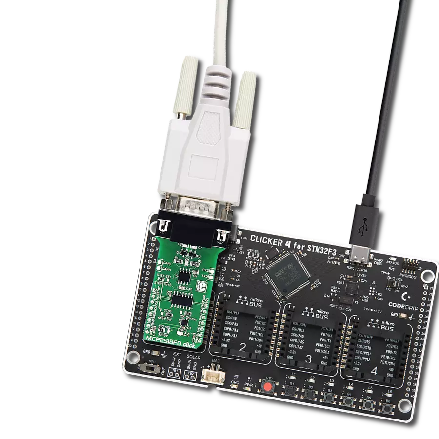
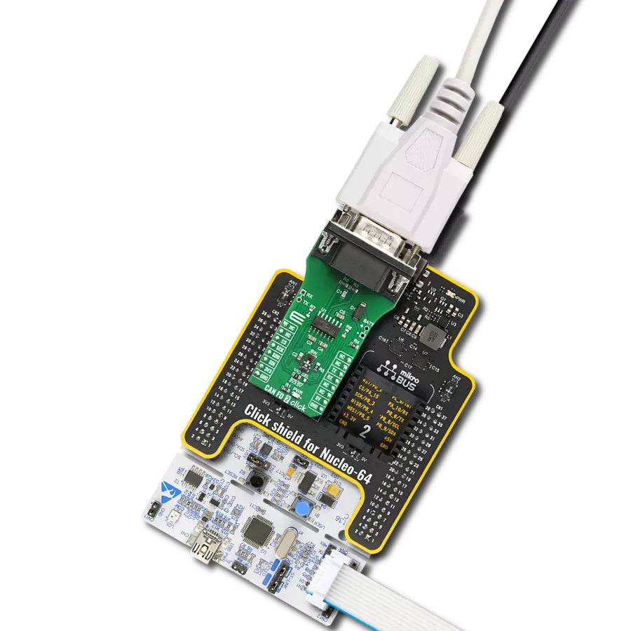
CAN FD 4 Click
Dev. board
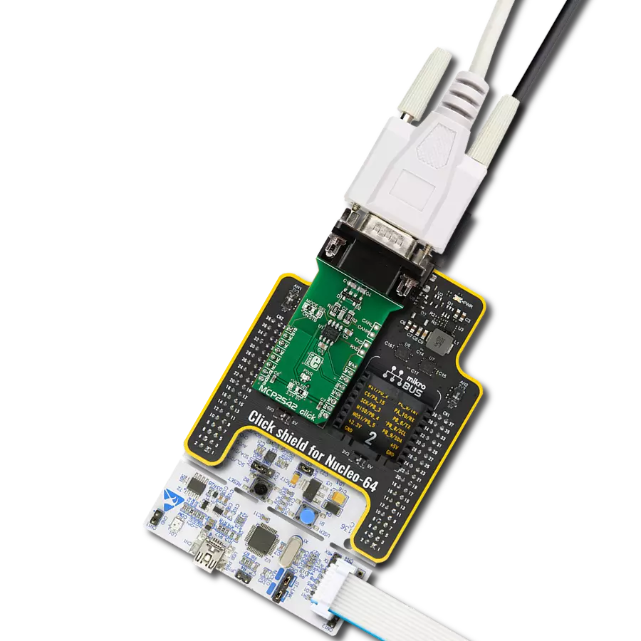
Nucleo 64 with STM32F410RB MCU
Compiler
NECTO Studio
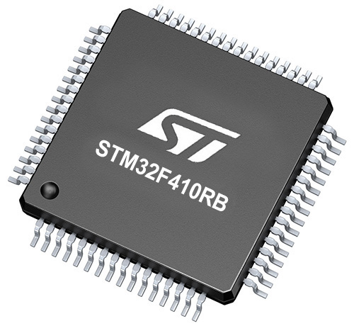
MCU
STM32F410RB
Future-proof your automotive network with our advanced high-speed CAN FD transceiver solution
A
A
Hardware Overview
How does it work?
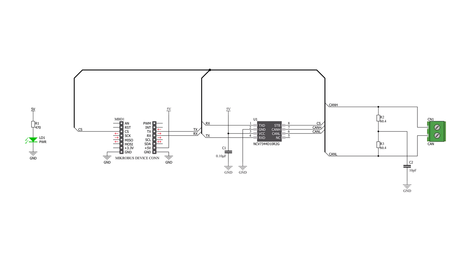
CAN FD 4 Click is based on the NCV7344, a complete CAN protocol controller, and the physical bus from ON Semiconductor. The Click board™ guarantees additional timing parameters to ensure robust communication at data rates beyond 1 Mbps to cope with CAN flexible data rate requirements (CAN FD). These features make the CAN FD 4 click a good choice for all high speed - controller area network (HS−CAN) networks. The CAN FD 4 click provides two operation modes: selectable pin CS. The first option is normal mode (when the CS pin is LOW), where the transceiver can communicate via the bus line. The CAN controller transmits and receives the signals via
the pins TxD and RxD. The slopes on the bus line outputs are optimized to give low EME. The second option is when the CS pin is HIGH and the CAN FD 4 click is in Standby mode. In standby mode, both the transmitter and receiver are disabled, and a very low−power differential receiver monitors the bus lines for CAN bus activity. When the low−power differential receiver detects a wake−up request, the signal is first filtered and then verified as a valid wake signal after a time period of twake_filt; the RxD pin is driven low by the transceiver (following the bus) to inform the controller of the wake−up request. High-speed CAN (HS CAN) is a serial bus system
that connects microcontrollers, sensors, and actuators for real-time control applications. Compatible with ISO 11898-2 (2016) describes using the Controller Area Network (CAN) within road vehicles. According to the 7-layer OSI reference model, the physical layer of an HS CAN bus system specifies the data transmission from one CAN node to all other available CAN nodes within the network. The CAN transceiver is part of the physical layer. This Click board™ is designed to be operated only with a 5V logic level. A proper logic voltage level conversion should be performed before the Click board™ is used with MCUs with logic levels of 3.3V.


Features overview
Development board
Nucleo-64 with STM32F410RB MCU offers a cost-effective and adaptable platform for developers to explore new ideas and prototype their designs. This board harnesses the versatility of the STM32 microcontroller, enabling users to select the optimal balance of performance and power consumption for their projects. It accommodates the STM32 microcontroller in the LQFP64 package and includes essential components such as a user LED, which doubles as an ARDUINO® signal, alongside user and reset push-buttons, and a 32.768kHz crystal oscillator for precise timing operations. Designed with expansion and flexibility in mind, the Nucleo-64 board features an ARDUINO® Uno V3 expansion connector and ST morpho extension pin
headers, granting complete access to the STM32's I/Os for comprehensive project integration. Power supply options are adaptable, supporting ST-LINK USB VBUS or external power sources, ensuring adaptability in various development environments. The board also has an on-board ST-LINK debugger/programmer with USB re-enumeration capability, simplifying the programming and debugging process. Moreover, the board is designed to simplify advanced development with its external SMPS for efficient Vcore logic supply, support for USB Device full speed or USB SNK/UFP full speed, and built-in cryptographic features, enhancing both the power efficiency and security of projects. Additional connectivity is
provided through dedicated connectors for external SMPS experimentation, a USB connector for the ST-LINK, and a MIPI® debug connector, expanding the possibilities for hardware interfacing and experimentation. Developers will find extensive support through comprehensive free software libraries and examples, courtesy of the STM32Cube MCU Package. This, combined with compatibility with a wide array of Integrated Development Environments (IDEs), including IAR Embedded Workbench®, MDK-ARM, and STM32CubeIDE, ensures a smooth and efficient development experience, allowing users to fully leverage the capabilities of the Nucleo-64 board in their projects.

Microcontroller Overview
MCU Card / MCU
Architecture
ARM Cortex-M4
MCU Memory (KB)
128
Silicon Vendor
STMicroelectronics
Pin count
64
RAM (Bytes)
32768
You complete me!
Accessories
Click Shield for Nucleo-64 comes equipped with two proprietary mikroBUS™ sockets, allowing all the Click board™ devices to be interfaced with the STM32 Nucleo-64 board with no effort. This way, Mikroe allows its users to add any functionality from our ever-growing range of Click boards™, such as WiFi, GSM, GPS, Bluetooth, ZigBee, environmental sensors, LEDs, speech recognition, motor control, movement sensors, and many more. More than 1537 Click boards™, which can be stacked and integrated, are at your disposal. The STM32 Nucleo-64 boards are based on the microcontrollers in 64-pin packages, a 32-bit MCU with an ARM Cortex M4 processor operating at 84MHz, 512Kb Flash, and 96KB SRAM, divided into two regions where the top section represents the ST-Link/V2 debugger and programmer while the bottom section of the board is an actual development board. These boards are controlled and powered conveniently through a USB connection to program and efficiently debug the Nucleo-64 board out of the box, with an additional USB cable connected to the USB mini port on the board. Most of the STM32 microcontroller pins are brought to the IO pins on the left and right edge of the board, which are then connected to two existing mikroBUS™ sockets. This Click Shield also has several switches that perform functions such as selecting the logic levels of analog signals on mikroBUS™ sockets and selecting logic voltage levels of the mikroBUS™ sockets themselves. Besides, the user is offered the possibility of using any Click board™ with the help of existing bidirectional level-shifting voltage translators, regardless of whether the Click board™ operates at a 3.3V or 5V logic voltage level. Once you connect the STM32 Nucleo-64 board with our Click Shield for Nucleo-64, you can access hundreds of Click boards™, working with 3.3V or 5V logic voltage levels.

Used MCU Pins
mikroBUS™ mapper
Take a closer look
Click board™ Schematic
Step by step
Project assembly
Start by selecting your development board and Click board™. Begin with the Nucleo 64 with STM32F410RB MCU as your development board.


Software Support
Library Description
This library contains API for CAN FD 4 Click driver.
Key functions:
canfd4_generic_write- Generic write functioncanfd4_set_dev_mode- Set mode functioncanfd4_generic_read- Generic read function
Open Source
Code example
The complete application code and a ready-to-use project are available through the NECTO Studio Package Manager for direct installation in the NECTO Studio. The application code can also be found on the MIKROE GitHub account.
/*!
 * \file
 * \brief CanFd4 Click example
 *
 * # Description
 * This example reads and processes data from CAN FD 4 Clicks.
 *
 * The demo application is composed of two sections :
 *
 * ## Application Init
 * Initializes the driver and enables the Click board.
 *
 * ## Application Task
 * Depending on the selected mode, it reads all the received data or sends the desired message
 * every 2 seconds.
 *
 * ## Additional Function
 * - canfd4_process ( ) - The general process of collecting the received data.
 *
 *
 * \author MikroE Team
 *
 */
// ------------------------------------------------------------------- INCLUDES

#include "board.h"
#include "log.h"
#include "canfd4.h"
#include "string.h"

#define PROCESS_RX_BUFFER_SIZE 500

#define TEXT_TO_SEND "MikroE\r\n"

// ------------------------------------------------------------------ VARIABLES

#define DEMO_APP_RECEIVER
// #define DEMO_APP_TRANSMITTER

static canfd4_t canfd4;
static log_t logger;

// ------------------------------------------------------- ADDITIONAL FUNCTIONS

static void canfd4_process ( void )
{
    int32_t rsp_size;

    char uart_rx_buffer[ PROCESS_RX_BUFFER_SIZE ] = { 0 };
    uint8_t check_buf_cnt;

    rsp_size = canfd4_generic_read( &canfd4, uart_rx_buffer, PROCESS_RX_BUFFER_SIZE );

    if ( rsp_size > 6 )
    {
        log_printf( &logger, "Received data: " );

        for ( check_buf_cnt = 0; check_buf_cnt < rsp_size; check_buf_cnt++ )
        {
            log_printf( &logger, "%c", uart_rx_buffer[ check_buf_cnt ] );
        }
    }
    Delay_ms ( 100 );
}

// ------------------------------------------------------ APPLICATION FUNCTIONS

void application_init ( void )
{
    log_cfg_t log_cfg;
    canfd4_cfg_t cfg;

    /**
     * Logger initialization.
     * Default baud rate: 115200
     * Default log level: LOG_LEVEL_DEBUG
     * @note If USB_UART_RX and USB_UART_TX
     * are defined as HAL_PIN_NC, you will
     * need to define them manually for log to work.
     * See @b LOG_MAP_USB_UART macro definition for detailed explanation.
     */
    LOG_MAP_USB_UART( log_cfg );
    log_init( &logger, &log_cfg );
    log_info( &logger, "---- Application Init ----" );

    //  Click initialization.

    canfd4_cfg_setup( &cfg );
    CANFD4_MAP_MIKROBUS( cfg, MIKROBUS_1 );
    canfd4_init( &canfd4, &cfg );

    canfd4_set_dev_mode ( &canfd4, CANFD4_NORMAL_MODE );
    Delay_ms ( 100 );
}

void application_task ( void )
{
#ifdef DEMO_APP_RECEIVER
    canfd4_process( );
#endif
#ifdef DEMO_APP_TRANSMITTER
    canfd4_generic_write( &canfd4, TEXT_TO_SEND, 8 );
    log_info( &logger, "--- The message is sent ---" );
    Delay_ms ( 1000 );
    Delay_ms ( 1000 );
#endif
}

int main ( void )
{
    /* Do not remove this line or clock might not be set correctly. */
    #ifdef PREINIT_SUPPORTED
    preinit();
    #endif

    application_init( );

    for ( ; ; )
    {
        application_task( );
    }

    return 0;
}


// ------------------------------------------------------------------------ END
Additional Support
Resources
Category:CAN