Utilize TLE7268 and STM32F091RC to simplify automotive networking
Streamlined communication: Unleash the potential of LIN transceivers
Published Feb 26, 2024
Click board™
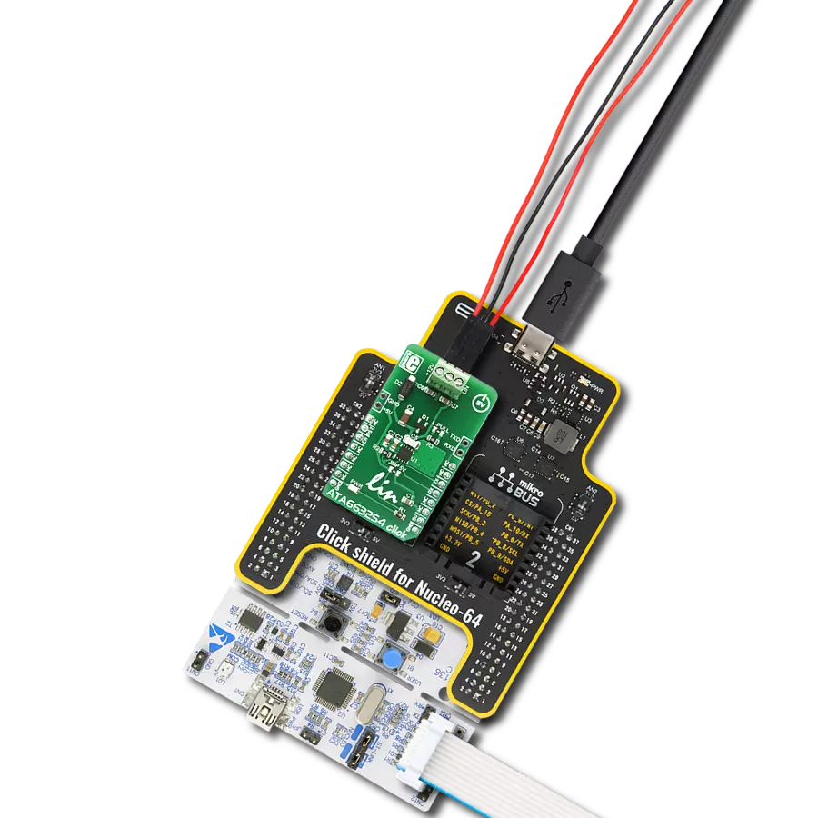
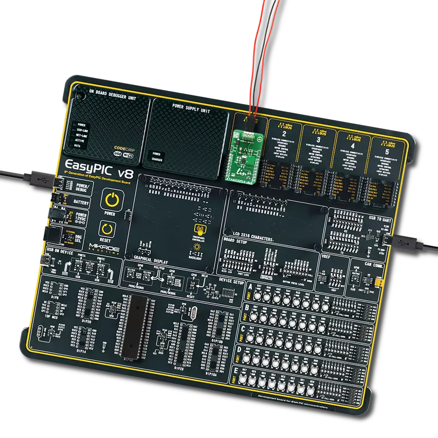
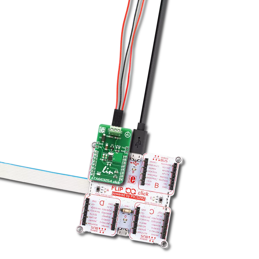
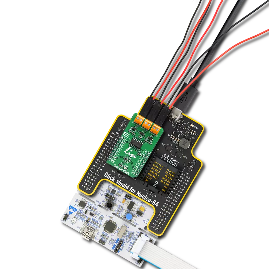
Dual LIN Click
Dev. board
Nucleo-64 with STM32F091RC MCU
Compiler
NECTO Studio
MCU
STM32F091RC
Our LIN transceivers offer unwavering reliability for data exchange in vehicles and industrial systems, contributing to safer and more efficient journeys
A
A
Hardware Overview
How does it work?
Dual LIN Click is based on the TLE7268, a dual transceiver for the Local Interconnect Network (LIN) from Infineon with integrated wake-up and protection features. The Dual LIN click is designed for in-vehicle networks using data transmission rates up to 20 kbps. Dual LIN click includes two independent transceivers that operate as bus drivers between the protocol controller and physical LIN networks. The Dual LIN click communicates with the MCU by using the UART RX and TX signals. RX and TX signals are also routed to the header on the edge of the click board™ so they can be used independently of the mikroBUS™ socket. Its most important features are the fact that it is a two separate single-wire LIN transceiver bus for transmission rates up to 20 kbps and it is compliant to ISO 17987-4 and LIN Specification 2.2A. The EN1 and EN2 pins are used to enable the functionality of BUS 1 or BUS 2 of the device. When the EN1 pin is set to a HIGH logic level, the BUS 1 of the device is set to work in the normal mode, with the transmission paths from TXD to LIN and from LIN to RXD both active. When
the EN2 pin is set to a HIGH logic level, the BUS 2 of the device is set to work in the normal mode, with the transmission paths from TXD to LIN and from LIN to RXD both active. When the EN1 pin is set to a LOW state, the BUS 1 of the device is put into silent mode, depending on the TX pin state. The EN1 pin has a pull-down resistor, so it is pulled to Ground if it is left afloat. When the EN2 pin is set to a LOW state, the BUS 2 of the device is put into silent mode, depending on the TX pin state. The EN2 pin has a pull-down resistor, so it is pulled to Ground if it is left afloat. The Dual LIN click supports different modes of operation of the two transceivers for minimizing ECU current consumption in low power modes, a common INH output can be used for controlling external circuitry, for example voltage regulators. Based on the Infineon BiCMOS technology. It provides excellent ESD robustness together with very high electromagnetic compliance (EMC). The TLE7268 reaches a very low level of electromagnetic emission (EME) within a broad frequency range and independent from the battery voltage. The
TLE7268 is AEC qualified and tailored to withstand the harsh conditions of the automotive environment. Some of the key features that are incorporated in the TLE7268 are overtemperature protection, undervoltage detection. The Dual LIN click is digital I/O levels compatible with 3.3 V and 5 V microcontrollers, that it is optimized for high electromagnetic compliance (EMC) with very low electromagnetic emission and high immunity to interference. It also features two independent single-wire LIN transceivers in one device and gives out a transmission rate of up to 20 kbps. Given the features included in this transceiver, the Dual LIN click can be used for Body Control Modules (BCM) and Gateway. This Click board™ can operate with either 3.3V or 5V logic voltage levels selected via the VCC SEL jumper. This way, both 3.3V and 5V capable MCUs can use the communication lines properly. Also, this Click board™ comes equipped with a library containing easy-to-use functions and an example code that can be used as a reference for further development.

Features overview
Development board
Nucleo-64 with STM32F091RC MCU offers a cost-effective and adaptable platform for developers to explore new ideas and prototype their designs. This board harnesses the versatility of the STM32 microcontroller, enabling users to select the optimal balance of performance and power consumption for their projects. It accommodates the STM32 microcontroller in the LQFP64 package and includes essential components such as a user LED, which doubles as an ARDUINO® signal, alongside user and reset push-buttons, and a 32.768kHz crystal oscillator for precise timing operations. Designed with expansion and flexibility in mind, the Nucleo-64 board features an ARDUINO® Uno V3 expansion connector and ST morpho extension pin
headers, granting complete access to the STM32's I/Os for comprehensive project integration. Power supply options are adaptable, supporting ST-LINK USB VBUS or external power sources, ensuring adaptability in various development environments. The board also has an on-board ST-LINK debugger/programmer with USB re-enumeration capability, simplifying the programming and debugging process. Moreover, the board is designed to simplify advanced development with its external SMPS for efficient Vcore logic supply, support for USB Device full speed or USB SNK/UFP full speed, and built-in cryptographic features, enhancing both the power efficiency and security of projects. Additional connectivity is
provided through dedicated connectors for external SMPS experimentation, a USB connector for the ST-LINK, and a MIPI® debug connector, expanding the possibilities for hardware interfacing and experimentation. Developers will find extensive support through comprehensive free software libraries and examples, courtesy of the STM32Cube MCU Package. This, combined with compatibility with a wide array of Integrated Development Environments (IDEs), including IAR Embedded Workbench®, MDK-ARM, and STM32CubeIDE, ensures a smooth and efficient development experience, allowing users to fully leverage the capabilities of the Nucleo-64 board in their projects.

Microcontroller Overview
MCU Card / MCU

Architecture
ARM Cortex-M0
MCU Memory (KB)
256
Silicon Vendor
STMicroelectronics
Pin count
64
RAM (Bytes)
32768
You complete me!
Accessories
Click Shield for Nucleo-64 comes equipped with two proprietary mikroBUS™ sockets, allowing all the Click board™ devices to be interfaced with the STM32 Nucleo-64 board with no effort. This way, Mikroe allows its users to add any functionality from our ever-growing range of Click boards™, such as WiFi, GSM, GPS, Bluetooth, ZigBee, environmental sensors, LEDs, speech recognition, motor control, movement sensors, and many more. More than 1537 Click boards™, which can be stacked and integrated, are at your disposal. The STM32 Nucleo-64 boards are based on the microcontrollers in 64-pin packages, a 32-bit MCU with an ARM Cortex M4 processor operating at 84MHz, 512Kb Flash, and 96KB SRAM, divided into two regions where the top section represents the ST-Link/V2 debugger and programmer while the bottom section of the board is an actual development board. These boards are controlled and powered conveniently through a USB connection to program and efficiently debug the Nucleo-64 board out of the box, with an additional USB cable connected to the USB mini port on the board. Most of the STM32 microcontroller pins are brought to the IO pins on the left and right edge of the board, which are then connected to two existing mikroBUS™ sockets. This Click Shield also has several switches that perform functions such as selecting the logic levels of analog signals on mikroBUS™ sockets and selecting logic voltage levels of the mikroBUS™ sockets themselves. Besides, the user is offered the possibility of using any Click board™ with the help of existing bidirectional level-shifting voltage translators, regardless of whether the Click board™ operates at a 3.3V or 5V logic voltage level. Once you connect the STM32 Nucleo-64 board with our Click Shield for Nucleo-64, you can access hundreds of Click boards™, working with 3.3V or 5V logic voltage levels.

Used MCU Pins
mikroBUS™ mapper
Take a closer look
Click board™ Schematic

Step by step
Project assembly
Start by selecting your development board and Click board™. Begin with the Nucleo-64 with STM32F091RC MCU as your development board.


Software Support
Library Description
This library contains API for Dual LIN Click driver.
Key functions:
duallin_bus1_status- Sets state of RST pinduallin_bus2_status- Sets state of CS pinduallin_send_command- Send command.
Open Source
Code example
The complete application code and a ready-to-use project are available through the NECTO Studio Package Manager for direct installation in the NECTO Studio. The application code can also be found on the MIKROE GitHub account.
/*!
 * \file
 * \brief DualLin Click example
 *
 * # Description
 * This example reads and processes data from Dual LIN Clicks.
 *
 * The demo application is composed of two sections :
 *
 * ## Application Init
 * Initializes driver, and sets bus.
 *
 * ## Application Task
 * Reads the received data.
 *
 * ## Additional Function
 * - duallin_process ( ) - The general process of collecting presponce
 *                                   that sends a module.
 *
 * \author MikroE Team
 *
 */
// ------------------------------------------------------------------- INCLUDES

#include "board.h"
#include "log.h"
#include "duallin.h"
#include "string.h"

#define PROCESS_COUNTER 10
#define PROCESS_RX_BUFFER_SIZE 500

#define TEXT_TO_SEND "MikroE\r\n"

// ------------------------------------------------------------------ VARIABLES

#define DEMO_APP_RECEIVER
// #define DEMO_APP_TRANSMITER

static duallin_t duallin;
static log_t logger;

static char current_rsp_buf[ PROCESS_RX_BUFFER_SIZE ];

// ------------------------------------------------------ APPLICATION FUNCTIONS

void application_init ( void )
{
    log_cfg_t log_cfg;
    duallin_cfg_t cfg;

    /**
     * Logger initialization.
     * Default baud rate: 115200
     * Default log level: LOG_LEVEL_DEBUG
     * @note If USB_UART_RX and USB_UART_TX
     * are defined as HAL_PIN_NC, you will
     * need to define them manually for log to work.
     * See @b LOG_MAP_USB_UART macro definition for detailed explanation.
     */
    LOG_MAP_USB_UART( log_cfg );
    log_init( &logger, &log_cfg );
    log_info( &logger, "---- Application Init ----" );

    //  Click initialization.

    duallin_cfg_setup( &cfg );
    DUALLIN_MAP_MIKROBUS( cfg, MIKROBUS_1 );
    duallin_init( &duallin, &cfg );

    duallin_bus1_status( &duallin, DUALLIN_PIN_STATE_HIGH );
    duallin_bus2_status( &duallin, DUALLIN_PIN_STATE_LOW );
    Delay_ms ( 100 );
}

void application_task ( void )
{
#ifdef DEMO_APP_RECEIVER
    int32_t rsp_size = duallin_generic_read( &duallin, current_rsp_buf, PROCESS_RX_BUFFER_SIZE );
    if ( rsp_size> 0)
    {
        log_printf( &logger, "%s", current_rsp_buf );
    }
#endif

#ifdef DEMO_APP_TRANSMITER
    duallin_send_command( &duallin, TEXT_TO_SEND );
    Delay_ms ( 1000 );
    Delay_ms ( 1000 );
#endif
}

int main ( void )
{
    /* Do not remove this line or clock might not be set correctly. */
    #ifdef PREINIT_SUPPORTED
    preinit();
    #endif

    application_init( );

    for ( ; ; )
    {
        application_task( );
    }

    return 0;
}

// ------------------------------------------------------------------------ END
Additional Support
Resources
Category:LIN