Enhance system performance with high-speed flash storage using IS25LP128 and STM32G071RB
Embrace the future with flash storage

Published Oct 08, 2024
Click board™
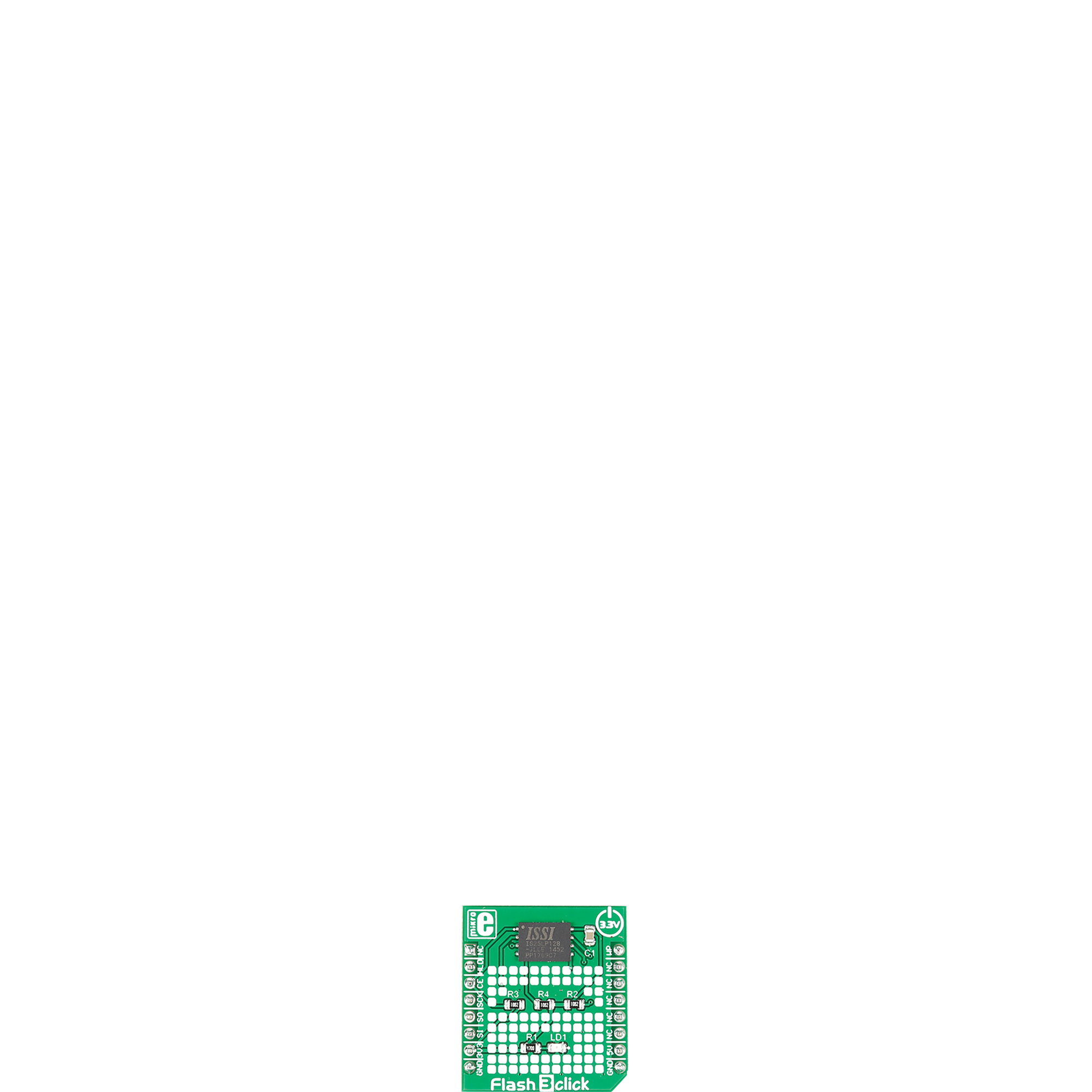
Flash 3 Click
Dev. board
Nucleo 64 with STM32G071RB MCU
Compiler
NECTO Studio
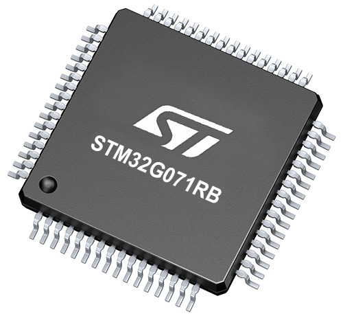
MCU
STM32G071RB
Employ flash memory to boost overall system responsiveness and application loading times
A
A
Hardware Overview
How does it work?
Flash 3 Click is based on the IS25LP128, a serial Flash memory with 133MHz multi I/O SPI & quad I/O QPI DTR interfaces from Integrated Silicon Solution. This Flash memory chip supports Serial Flash Discoverable Parameters (SFDP), selectable dummy cycles, SPI modes 0 and 3, and configurable drive strength. The flexible and efficient memory architecture allows chip erase with uniform sector/block erase (4/32/64 KB) and program/erase suspend and resume. The read and program modes consist of low instruction overhead operations, continuous read 8/16/32/64-byte burst wrap, selectable burst length,
and more. There are software and hardware protections, power supply lock protection, a 4x256-byte dedicated security area with OTP user-lockable bits, and the 128-bit Unique ID for each device. The Flash 3 Click communicates with the host MCU through an industry-standard SPI serial interface, supporting the two most common SPI modes, SPI Mode 0 and 3, with a maximum frequency of 133MHz in Fast Read mode. The Flash 3 Click features write-protect ability over the WP pin, with active LOW. The HLD pin is a communication hold pin, and the Flash memory can stay in a hold state with logic LOW, in which
time the device is paused without resetting the serial sequence. The CE pin turns the device’s operation on and off on this Click board™, pulled high for normal operation. This Click board™ can be operated only with a 3.3V logic voltage level. The board must perform appropriate logic voltage level conversion before using MCUs with different logic levels. Also, it comes equipped with a library containing functions and an example code that can be used, as a reference, for further development.


Features overview
Development board
Nucleo-64 with STM32G071RB MCU offers a cost-effective and adaptable platform for developers to explore new ideas and prototype their designs. This board harnesses the versatility of the STM32 microcontroller, enabling users to select the optimal balance of performance and power consumption for their projects. It accommodates the STM32 microcontroller in the LQFP64 package and includes essential components such as a user LED, which doubles as an ARDUINO® signal, alongside user and reset push-buttons, and a 32.768kHz crystal oscillator for precise timing operations. Designed with expansion and flexibility in mind, the Nucleo-64 board features an ARDUINO® Uno V3 expansion connector and ST morpho extension pin
headers, granting complete access to the STM32's I/Os for comprehensive project integration. Power supply options are adaptable, supporting ST-LINK USB VBUS or external power sources, ensuring adaptability in various development environments. The board also has an on-board ST-LINK debugger/programmer with USB re-enumeration capability, simplifying the programming and debugging process. Moreover, the board is designed to simplify advanced development with its external SMPS for efficient Vcore logic supply, support for USB Device full speed or USB SNK/UFP full speed, and built-in cryptographic features, enhancing both the power efficiency and security of projects. Additional connectivity is
provided through dedicated connectors for external SMPS experimentation, a USB connector for the ST-LINK, and a MIPI® debug connector, expanding the possibilities for hardware interfacing and experimentation. Developers will find extensive support through comprehensive free software libraries and examples, courtesy of the STM32Cube MCU Package. This, combined with compatibility with a wide array of Integrated Development Environments (IDEs), including IAR Embedded Workbench®, MDK-ARM, and STM32CubeIDE, ensures a smooth and efficient development experience, allowing users to fully leverage the capabilities of the Nucleo-64 board in their projects.

Microcontroller Overview
MCU Card / MCU
Architecture
ARM Cortex-M0
MCU Memory (KB)
128
Silicon Vendor
STMicroelectronics
Pin count
64
RAM (Bytes)
36864
You complete me!
Accessories
Click Shield for Nucleo-64 comes equipped with two proprietary mikroBUS™ sockets, allowing all the Click board™ devices to be interfaced with the STM32 Nucleo-64 board with no effort. This way, Mikroe allows its users to add any functionality from our ever-growing range of Click boards™, such as WiFi, GSM, GPS, Bluetooth, ZigBee, environmental sensors, LEDs, speech recognition, motor control, movement sensors, and many more. More than 1537 Click boards™, which can be stacked and integrated, are at your disposal. The STM32 Nucleo-64 boards are based on the microcontrollers in 64-pin packages, a 32-bit MCU with an ARM Cortex M4 processor operating at 84MHz, 512Kb Flash, and 96KB SRAM, divided into two regions where the top section represents the ST-Link/V2 debugger and programmer while the bottom section of the board is an actual development board. These boards are controlled and powered conveniently through a USB connection to program and efficiently debug the Nucleo-64 board out of the box, with an additional USB cable connected to the USB mini port on the board. Most of the STM32 microcontroller pins are brought to the IO pins on the left and right edge of the board, which are then connected to two existing mikroBUS™ sockets. This Click Shield also has several switches that perform functions such as selecting the logic levels of analog signals on mikroBUS™ sockets and selecting logic voltage levels of the mikroBUS™ sockets themselves. Besides, the user is offered the possibility of using any Click board™ with the help of existing bidirectional level-shifting voltage translators, regardless of whether the Click board™ operates at a 3.3V or 5V logic voltage level. Once you connect the STM32 Nucleo-64 board with our Click Shield for Nucleo-64, you can access hundreds of Click boards™, working with 3.3V or 5V logic voltage levels.

Used MCU Pins
mikroBUS™ mapper
Take a closer look
Click board™ Schematic

Step by step
Project assembly
Start by selecting your development board and Click board™. Begin with the Nucleo 64 with STM32G071RB MCU as your development board.


Software Support
Library Description
This library contains API for Flash 3 Click driver.
Key functions:
flash3_pause- Pause functionflash3_unpause- Unpause function
Open Source
Code example
The complete application code and a ready-to-use project are available through the NECTO Studio Package Manager for direct installation in the NECTO Studio. The application code can also be found on the MIKROE GitHub account.
/*!
 * \file
 * \brief Flash3 Click example
 *
 * # Description
 * This applicaion adding more flash memory.
 *
 * The demo application is composed of two sections :
 *
 * ## Application Init
 * Initalizes device, Flash 3 Click board and makes an initial log.
 *
 * ## Application Task
 * This is an example that shows the capabilities of the Flash 3 Click by
   writing into memory array of a Flash 3 Click board and reading same data from memory array.
 *
 * \author MikroE Team
 *
 */
// ------------------------------------------------------------------- INCLUDES

#include "board.h"
#include "log.h"
#include "flash3.h"

// ------------------------------------------------------------------ VARIABLES

static flash3_t flash3;
static log_t logger;

// ------------------------------------------------------ APPLICATION FUNCTIONS

void application_init ( void )
{
    log_cfg_t log_cfg;
    flash3_cfg_t cfg;

    /**
     * Logger initialization.
     * Default baud rate: 115200
     * Default log level: LOG_LEVEL_DEBUG
     * @note If USB_UART_RX and USB_UART_TX
     * are defined as HAL_PIN_NC, you will
     * need to define them manually for log to work.
     * See @b LOG_MAP_USB_UART macro definition for detailed explanation.
     */
    LOG_MAP_USB_UART( log_cfg );
    log_init( &logger, &log_cfg );
    log_info( &logger, "---- Application Init ----" );

    //  Click initialization.

    flash3_cfg_setup( &cfg );
    FLASH3_MAP_MIKROBUS( cfg, MIKROBUS_1 );
    flash3_init( &flash3, &cfg );

    Delay_ms ( 100 );
    log_printf( &logger, "------------------- \r\n" );
    log_printf( &logger, "  Flash  3  Click  \r\n" );
    log_printf( &logger, "-------------------\r\n" );
    flash3_setting( &flash3 );
    Delay_ms ( 100 );
    log_printf( &logger, "   Initialized     \r\n" );
    log_printf( &logger, "------------------- \r\n" );
}

void application_task ( void )
{
    char val_in[ 8 ] = { 0x4D, 0x49, 0x4B, 0x52, 0x4F, 0x45, 0x00 };
    char val_out[ 8 ] = { 0 };

    log_printf( &logger, "\r\n ____________________ \r\n" );
    log_printf( &logger, "Begin demonstration! \r\n\r\n" );


    log_printf( &logger, "Writing : %s\r\n", val_in );
    flash3_write( &flash3, 0x000000, &val_in[ 0 ], 6 );
    Delay_ms ( 100 );
    log_printf( &logger, "------------------ \r\n" );

    log_printf( &logger, "Reading : %s\r\n", val_in );
    flash3_normal_read( &flash3, 0x000000, &val_in[ 0 ], 6 );
    Delay_ms ( 100 );
    log_printf( &logger, "------------------ \r\n" );

    log_printf( &logger, "Erasing... \r\n" );
    flash3_sector_erase( &flash3, 0x000000 );
    Delay_ms ( 300 );
    log_printf( &logger, "Erased!" );
    Delay_ms ( 100 );
    log_printf( &logger, "------------------ \r\n"  );

    log_printf( &logger, "Reading : %s\r\n", val_out );
    flash3_fast_read( &flash3, 0x000000, &val_out[ 0 ], 6 );
    Delay_ms ( 100 );
    log_printf( &logger, "------------------ \r\n" );

    log_printf( &logger, "Demonstration over!" );
    log_printf( &logger, "\r\n ___________________ \r\n" );
    Delay_ms ( 1000 );
    Delay_ms ( 1000 );
    Delay_ms ( 1000 );
    Delay_ms ( 1000 );
    Delay_ms ( 1000 );

}

int main ( void )
{
    /* Do not remove this line or clock might not be set correctly. */
    #ifdef PREINIT_SUPPORTED
    preinit();
    #endif

    application_init( );

    for ( ; ; )
    {
        application_task( );
    }

    return 0;
}


// ------------------------------------------------------------------------ END
Additional Support
Resources
Category:FLASH


