Accelerate data access and retrieval like never before with W25Q128JV and STM32F091RC
Flash forward to excellence

Published Feb 26, 2024
Click board™
Flash 6 Click
Dev. board
Nucleo-64 with STM32F091RC MCU
Compiler
NECTO Studio
MCU
STM32F091RC
Upgrade to faster, reliable storage with our flash memory solution
A
A
Hardware Overview
How does it work?
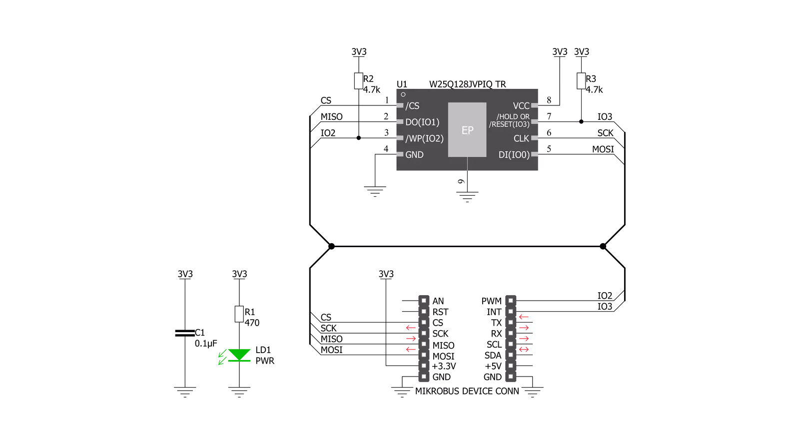
Flash 6 Click is based on the W25Q128JV, a 128M-bit flash memory from Winbond organized into 65,536 programmable pages of 256 bytes each. Up to 256 bytes can be programmed at a time. Pages can be erased in groups of 16 (4KB sector erase), groups of 128 (32KB block erase), groups of 256 (64KB block erase), or the entire chip (chip erase). The W25Q128JV has 4,096 erasable sectors and 256 erasable blocks respectively. The small 4KB sectors allow for greater flexibility in applications that require data and parameter storage. The Flash 6 Click uses the standard Serial Peripheral Interface (SPI), supporting SPI clock frequencies of up to 133MHz Single, Dual/Quad SPI clocks. Besides that, the W25Q128JV provides a Continuous Read Mode that allows for efficient access to the entire memory array with a single Read command. This feature is ideal for
code-shadowing applications. Also, it offers the highest performance thanks to 133MHz Standard/Dual/Quad SPI clocks and a 66MB/S continuous data transfer rate. It has an efficient Continuous Read Mode, allowing direct read access to the entire array. However, the performance depends on the main MCU used with this Click board™. A Hold pin, Write Protect pin and programmable write protection provide further control flexibility. Additionally, the device supports JEDEC standard manufacturer and device ID and SFDP, a 64-bit Unique Serial Number, and three 256-byte Security Registers. The W25Q128JV is accessed through an SPI-compatible bus consisting of four signals: Serial Clock (CLK), Chip Select (/CS), Serial Data Input (DI), and Serial Data Output (DO). Standard SPI instructions use the DI input pin to serially
write instructions, addresses, or data to the device on the rising edge of CLK. The DO output pin reads data or status from the device on the falling edge of CLK. For a detailed explanation, please consult the included datasheet. However, MIKROE provides a library that contains functions that simplify and speed up working with this device. The provided application example demonstrates the functionality of the library functions. It can be used as a reference for a custom project development. This Click board™ can be operated only with a 3.3V logic voltage level. The board must perform appropriate logic voltage level conversion before using MCUs with different logic levels. Also, it comes equipped with a library containing functions and an example code that can be used as a reference for further development.


Features overview
Development board
Nucleo-64 with STM32F091RC MCU offers a cost-effective and adaptable platform for developers to explore new ideas and prototype their designs. This board harnesses the versatility of the STM32 microcontroller, enabling users to select the optimal balance of performance and power consumption for their projects. It accommodates the STM32 microcontroller in the LQFP64 package and includes essential components such as a user LED, which doubles as an ARDUINO® signal, alongside user and reset push-buttons, and a 32.768kHz crystal oscillator for precise timing operations. Designed with expansion and flexibility in mind, the Nucleo-64 board features an ARDUINO® Uno V3 expansion connector and ST morpho extension pin
headers, granting complete access to the STM32's I/Os for comprehensive project integration. Power supply options are adaptable, supporting ST-LINK USB VBUS or external power sources, ensuring adaptability in various development environments. The board also has an on-board ST-LINK debugger/programmer with USB re-enumeration capability, simplifying the programming and debugging process. Moreover, the board is designed to simplify advanced development with its external SMPS for efficient Vcore logic supply, support for USB Device full speed or USB SNK/UFP full speed, and built-in cryptographic features, enhancing both the power efficiency and security of projects. Additional connectivity is
provided through dedicated connectors for external SMPS experimentation, a USB connector for the ST-LINK, and a MIPI® debug connector, expanding the possibilities for hardware interfacing and experimentation. Developers will find extensive support through comprehensive free software libraries and examples, courtesy of the STM32Cube MCU Package. This, combined with compatibility with a wide array of Integrated Development Environments (IDEs), including IAR Embedded Workbench®, MDK-ARM, and STM32CubeIDE, ensures a smooth and efficient development experience, allowing users to fully leverage the capabilities of the Nucleo-64 board in their projects.

Microcontroller Overview
MCU Card / MCU

Architecture
ARM Cortex-M0
MCU Memory (KB)
256
Silicon Vendor
STMicroelectronics
Pin count
64
RAM (Bytes)
32768
You complete me!
Accessories
Click Shield for Nucleo-64 comes equipped with two proprietary mikroBUS™ sockets, allowing all the Click board™ devices to be interfaced with the STM32 Nucleo-64 board with no effort. This way, Mikroe allows its users to add any functionality from our ever-growing range of Click boards™, such as WiFi, GSM, GPS, Bluetooth, ZigBee, environmental sensors, LEDs, speech recognition, motor control, movement sensors, and many more. More than 1537 Click boards™, which can be stacked and integrated, are at your disposal. The STM32 Nucleo-64 boards are based on the microcontrollers in 64-pin packages, a 32-bit MCU with an ARM Cortex M4 processor operating at 84MHz, 512Kb Flash, and 96KB SRAM, divided into two regions where the top section represents the ST-Link/V2 debugger and programmer while the bottom section of the board is an actual development board. These boards are controlled and powered conveniently through a USB connection to program and efficiently debug the Nucleo-64 board out of the box, with an additional USB cable connected to the USB mini port on the board. Most of the STM32 microcontroller pins are brought to the IO pins on the left and right edge of the board, which are then connected to two existing mikroBUS™ sockets. This Click Shield also has several switches that perform functions such as selecting the logic levels of analog signals on mikroBUS™ sockets and selecting logic voltage levels of the mikroBUS™ sockets themselves. Besides, the user is offered the possibility of using any Click board™ with the help of existing bidirectional level-shifting voltage translators, regardless of whether the Click board™ operates at a 3.3V or 5V logic voltage level. Once you connect the STM32 Nucleo-64 board with our Click Shield for Nucleo-64, you can access hundreds of Click boards™, working with 3.3V or 5V logic voltage levels.

Used MCU Pins
mikroBUS™ mapper
Take a closer look
Click board™ Schematic
Step by step
Project assembly
Start by selecting your development board and Click board™. Begin with the Nucleo-64 with STM32F091RC MCU as your development board.


Software Support
Library Description
This library contains API for Flash 6 Click driver.
Key functions:
flash6_write_memory_data- Function used for writing in memoryflash6_read_memory_data- Function used for reading from memoryflash6_erase_memory_segment- Function for eraseing segment
Open Source
Code example
The complete application code and a ready-to-use project are available through the NECTO Studio Package Manager for direct installation in the NECTO Studio. The application code can also be found on the MIKROE GitHub account.
/*!
 * \file
 * \brief Flash6 Click example
 *
 * # Description
 * This application writes in memory and reads from memory.
 *
 * The demo application is composed of two sections :
 *
 * ## Application Init
 * Initializes driver, resets device and tests communication.
 *
 * ## Application Task
 * Clears the memory sector, writes "MikroE" to device memory
 * and then reads it and sends it to log every 2 sec.
 *
 * \author MikroE Team
 *
 */
// ------------------------------------------------------------------- INCLUDES

#include "board.h"
#include "log.h"
#include "flash6.h"

// ------------------------------------------------------------------ VARIABLES

static flash6_t flash6;
static log_t logger;

static char write_buf[ 9 ] = { 'M', 'i', 'k', 'r', 'o', 'E', 13, 10, 0 };

// ------------------------------------------------------ APPLICATION FUNCTIONS

void application_init ( void )
{
    log_cfg_t log_cfg;
    flash6_cfg_t cfg;

    uint8_t manufacture_id;
    uint8_t device_id;

    /**
     * Logger initialization.
     * Default baud rate: 115200
     * Default log level: LOG_LEVEL_DEBUG
     * @note If USB_UART_RX and USB_UART_TX
     * are defined as HAL_PIN_NC, you will
     * need to define them manually for log to work.
     * See @b LOG_MAP_USB_UART macro definition for detailed explanation.
     */
    LOG_MAP_USB_UART( log_cfg );
    log_init( &logger, &log_cfg );
    log_info( &logger, "---- Application Init ----" );

    //  Click initialization.

    flash6_cfg_setup( &cfg );
    FLASH6_MAP_MIKROBUS( cfg, MIKROBUS_1 );
    flash6_init( &flash6, &cfg );

    flash6_software_reset( &flash6 );
    Delay_ms ( 100 );

    flash6_get_manufacture_device_id( &flash6, &manufacture_id, &device_id );
    log_printf( &logger, "\r\n ------> MANUFACTURE ID: 0x%x \r\n", manufacture_id );
    log_printf( &logger, " ------> DEVICE ID: 0x%x \r\n \r\n", device_id );
    Delay_ms ( 1000 );
}

void application_task ( void )
{
    uint32_t start_addr;
    char read_buff[ 50 ];
    uint8_t cnt;

    start_addr = 0x002000;

    log_printf( &logger, " ---> Erase sector  \r\n" );
    flash6_erase_memory_segment( &flash6, FLASH6_CMD_SECTOR_ERASE_4KB, start_addr );
    Delay_ms ( 500 );

    log_printf( &logger, " ---> Write in memory ... \r\n" );
    flash6_write_memory_data( &flash6, start_addr, &write_buf[ 0 ], 9 );
    log_printf( &logger, " ---> Read from memory \r\n" );
    flash6_read_memory_data( &flash6, start_addr, read_buff, 9 );

    log_printf( &logger, "---->>>> " );

    log_printf( &logger, "%s ", read_buff );
    Delay_ms ( 100 );
    log_printf( &logger, "----------------------------------\r\n" );

    Delay_ms ( 1000 );
    Delay_ms ( 1000 );
}

int main ( void )
{
    /* Do not remove this line or clock might not be set correctly. */
    #ifdef PREINIT_SUPPORTED
    preinit();
    #endif

    application_init( );

    for ( ; ; )
    {
        application_task( );
    }

    return 0;
}

// ------------------------------------------------------------------------ END
Additional Support
Resources
Category:FLASH


