Efficiently manage and retrieve your data with GD25LQ16C and STM32F446RE
Revolutionize your storage solution

Published Oct 08, 2024
Click board™
Flash 7 Click
Dev. board
Nucleo 64 with STM32F446RE MCU
Compiler
NECTO Studio
MCU
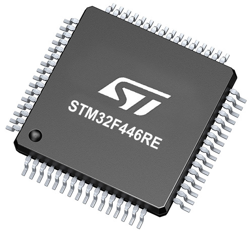
STM32F446RE
Enjoy rapid file transfers and smoother application performance
A
A
Hardware Overview
How does it work?
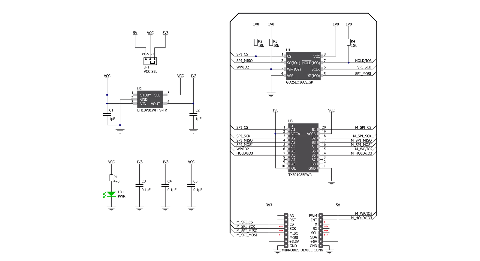
Flash 7 Click is based on the GD25LQ16C, a high-performance 16Mbit SPI NOR Flash Memory solution with advanced security features from GigaDevice Semiconductor. Requiring only six signals to communicate between the MCU and the memory thus reduces the design complexity board space and total system cost. It is specifically designed to meet the different needs of various electronic applications in terms of density, performance, reliability, and security while providing low power consumption. This Click board™ includes an LDO regulator BH18PB1WHFV from Rohm Semiconductor to provide the 1.8 V supply voltage. The LDO cuts power consumption by lowering its current consumption to approximately 2 μA when the application operates in the standby state. The output from the LDO
regulator provides a needed reference voltage for one side of the TXS0108E, an 8-bit bidirectional level shifting, and a voltage translator for open-drain and push-pull applications from Texas Instruments. The reference voltage for the other side of the level shifter is taken from the 3.3V pin from the mikroBUS™. Flash 7 Click communicates with MCU using the SPI serial interface that supports the Dual/Quad SPI and the two most common modes, SPI Mode 0 and 3, with a maximum SPI frequency of 104 MHz. The Dual I/O data is transferred with a speed of 208 Mbits/s, and the Quad I/O data with a speed of 416 Mbits/s. In addition to the SPI communication, the Flash 7 Click has two additional pins for Write Protection and HOLD function routed to the PWM and INT pins of the mikroBUS™ socket. The HOLD
pin, labeled as IO3, can be used to pause the serial communication with the device without stopping the operation of the write status register, programming, or erasing in progress. The configurable Write Protection function IO2 protects the memory array contents via the Software Protection Mode. This Click board™ can operate with either 3.3V or 5V logic voltage levels selected via the VCC SEL jumper. This way, both 3.3V and 5V capable MCUs can use the communication lines properly. Also, this Click board™ comes equipped with a library containing easy-to-use functions and an example code that can be used as a reference for further development.


Features overview
Development board
Nucleo-64 with STM32F446RE MCU offers a cost-effective and adaptable platform for developers to explore new ideas and prototype their designs. This board harnesses the versatility of the STM32 microcontroller, enabling users to select the optimal balance of performance and power consumption for their projects. It accommodates the STM32 microcontroller in the LQFP64 package and includes essential components such as a user LED, which doubles as an ARDUINO® signal, alongside user and reset push-buttons, and a 32.768kHz crystal oscillator for precise timing operations. Designed with expansion and flexibility in mind, the Nucleo-64 board features an ARDUINO® Uno V3 expansion connector and ST morpho extension pin
headers, granting complete access to the STM32's I/Os for comprehensive project integration. Power supply options are adaptable, supporting ST-LINK USB VBUS or external power sources, ensuring adaptability in various development environments. The board also has an on-board ST-LINK debugger/programmer with USB re-enumeration capability, simplifying the programming and debugging process. Moreover, the board is designed to simplify advanced development with its external SMPS for efficient Vcore logic supply, support for USB Device full speed or USB SNK/UFP full speed, and built-in cryptographic features, enhancing both the power efficiency and security of projects. Additional connectivity is
provided through dedicated connectors for external SMPS experimentation, a USB connector for the ST-LINK, and a MIPI® debug connector, expanding the possibilities for hardware interfacing and experimentation. Developers will find extensive support through comprehensive free software libraries and examples, courtesy of the STM32Cube MCU Package. This, combined with compatibility with a wide array of Integrated Development Environments (IDEs), including IAR Embedded Workbench®, MDK-ARM, and STM32CubeIDE, ensures a smooth and efficient development experience, allowing users to fully leverage the capabilities of the Nucleo-64 board in their projects.

Microcontroller Overview
MCU Card / MCU
Architecture
ARM Cortex-M4
MCU Memory (KB)
512
Silicon Vendor
STMicroelectronics
Pin count
64
RAM (Bytes)
131072
You complete me!
Accessories
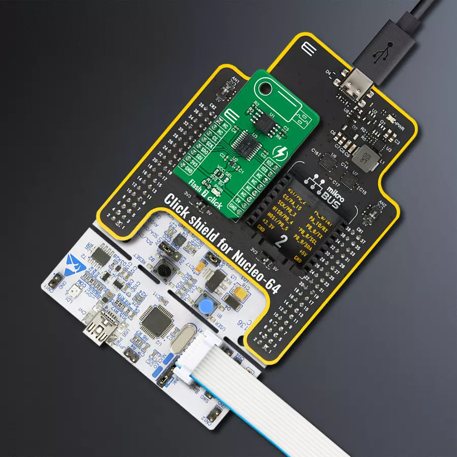
Click Shield for Nucleo-64 comes equipped with two proprietary mikroBUS™ sockets, allowing all the Click board™ devices to be interfaced with the STM32 Nucleo-64 board with no effort. This way, Mikroe allows its users to add any functionality from our ever-growing range of Click boards™, such as WiFi, GSM, GPS, Bluetooth, ZigBee, environmental sensors, LEDs, speech recognition, motor control, movement sensors, and many more. More than 1537 Click boards™, which can be stacked and integrated, are at your disposal. The STM32 Nucleo-64 boards are based on the microcontrollers in 64-pin packages, a 32-bit MCU with an ARM Cortex M4 processor operating at 84MHz, 512Kb Flash, and 96KB SRAM, divided into two regions where the top section represents the ST-Link/V2 debugger and programmer while the bottom section of the board is an actual development board. These boards are controlled and powered conveniently through a USB connection to program and efficiently debug the Nucleo-64 board out of the box, with an additional USB cable connected to the USB mini port on the board. Most of the STM32 microcontroller pins are brought to the IO pins on the left and right edge of the board, which are then connected to two existing mikroBUS™ sockets. This Click Shield also has several switches that perform functions such as selecting the logic levels of analog signals on mikroBUS™ sockets and selecting logic voltage levels of the mikroBUS™ sockets themselves. Besides, the user is offered the possibility of using any Click board™ with the help of existing bidirectional level-shifting voltage translators, regardless of whether the Click board™ operates at a 3.3V or 5V logic voltage level. Once you connect the STM32 Nucleo-64 board with our Click Shield for Nucleo-64, you can access hundreds of Click boards™, working with 3.3V or 5V logic voltage levels.

Used MCU Pins
mikroBUS™ mapper
Take a closer look
Click board™ Schematic
Step by step
Project assembly
Start by selecting your development board and Click board™. Begin with the Nucleo 64 with STM32F446RE MCU as your development board.


Software Support
Library Description
This library contains API for Flash 7 Click driver.
Key functions:
flash7_send_command- Send command functionflash7_page_program- Page program functionflash7_read_memory- Read memory function.
Open Source
Code example
The complete application code and a ready-to-use project are available through the NECTO Studio Package Manager for direct installation in the NECTO Studio. The application code can also be found on the MIKROE GitHub account.
/*!
 * @file main.c
 * @brief Flash7 Click example
 *
 * # Description
 * This is an example that demonstrates the use
 * of the Flash 7 Click board.
 *
 * The demo application is composed of two sections :
 *
 * ## Application Init
 * Initialization driver enables SPI,
 * disables write protect and hold, performs whole chip erase,
 * targets the memory address at "4096" for page program starting point
 * and writes data which is also displayed on the log.
 *
 * ## Application Task
 * In this example, the data is read from
 * the targeted memory address. The results are being sent to the Usart Terminal.
 * This task repeats every 5 sec.
 *
 * @author Stefan Ilic
 *
 */

#include "board.h"
#include "log.h"
#include "flash7.h"

static flash7_t flash7;
static log_t logger;

static char demo_data[ 9 ] = { 'm', 'i', 'k', 'r', 'o', 'E', 13 ,10 , 0 };
static char rx_data[ 9 ];
static uint32_t memory_addr;

void application_init ( void ) {
    log_cfg_t log_cfg;  /**< Logger config object. */
    flash7_cfg_t flash7_cfg;  /**< Click config object. */

    /**
     * Logger initialization.
     * Default baud rate: 115200
     * Default log level: LOG_LEVEL_DEBUG
     * @note If USB_UART_RX and USB_UART_TX
     * are defined as HAL_PIN_NC, you will
     * need to define them manually for log to work.
     * See @b LOG_MAP_USB_UART macro definition for detailed explanation.
     */
    LOG_MAP_USB_UART( log_cfg );
    log_init( &logger, &log_cfg );
    log_info( &logger, " Application Init " );

    // Click initialization.

    flash7_cfg_setup( &flash7_cfg );
    FLASH7_MAP_MIKROBUS( flash7_cfg, MIKROBUS_1 );
    err_t init_flag  = flash7_init( &flash7, &flash7_cfg );
    if ( SPI_MASTER_ERROR == init_flag ) {
        log_error( &logger, " Application Init Error. " );
        log_info( &logger, " Please, run program again... " );

        for ( ; ; );
    }

    flash7_default_cfg ( &flash7 );

    log_printf( &logger, " ----------------------- \r\n" );
    log_printf( &logger, " Chip Erase \r\n" );
    flash7_chip_erase( &flash7 );
    Delay_ms ( 1000 );
    Delay_ms ( 1000 );
    Delay_ms ( 1000 );
    Delay_ms ( 1000 );
    Delay_ms ( 1000 );

    memory_addr = 4096;

    log_printf( &logger, " ----------------------- \r\n" );
    log_printf( &logger, " Write data : %s ", demo_data );
    log_printf( &logger, " ----------------------- \r\n" );
    flash7_page_program( &flash7, memory_addr, demo_data, 9 );
    Delay_ms ( 100 );

    log_info( &logger, " Application Task " );
    log_printf( &logger, " ----------------------- \r\n" );
}

void application_task ( void ) {
    flash7_read_memory( &flash7, memory_addr, rx_data, 9 );
    log_printf( &logger, " Read data : %s ", rx_data );
    log_printf( &logger, " ----------------------- \r\n" );
    Delay_ms ( 1000 );
    Delay_ms ( 1000 );
    Delay_ms ( 1000 );
    Delay_ms ( 1000 );
    Delay_ms ( 1000 );
}

int main ( void )
{
    /* Do not remove this line or clock might not be set correctly. */
    #ifdef PREINIT_SUPPORTED
    preinit();
    #endif

    application_init( );

    for ( ; ; )
    {
        application_task( );
    }

    return 0;
}

// ------------------------------------------------------------------------ END
Additional Support
Resources
Category:FLASH


