Add data storage to any application with GD5F2GQ5UEYIGR and STM32F091RC
Improve your memory

Published Feb 26, 2024
Click board™
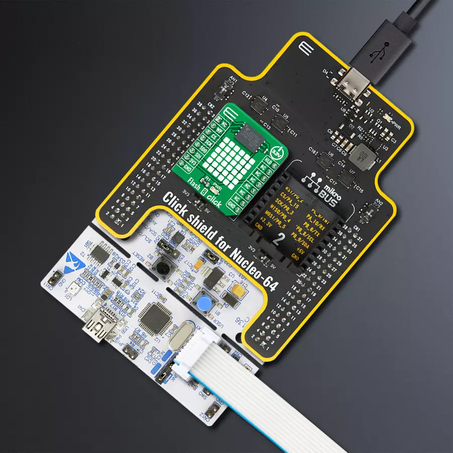
Flash 8 Click
Dev. board
Nucleo-64 with STM32F091RC MCU
Compiler
NECTO Studio
MCU
STM32F091RC
Highly reliable memory solution
A
A
Hardware Overview
How does it work?
Flash 8 Click is based on the GD5F2GQ5UEYIGR, a highly reliable serial Flash memory solution offering flexibility designed for use in various consumer applications from GigaDevice Semiconductor. It comes with a density of 2Gb based on an industry-standard NAND Flash memory core, representing an attractive alternative to SPI-NOR and standard parallel NAND Flash with advanced features. Organized as 256Mx8, the GD5F2GQ5UEYIGR has advanced security features (8K-Byte OTP region). It specifies a minimum of 100.000 endurance cycles with data retention of a minimum of 10 years, allowing it to handle unlimited reads/writes to the memory. This Click board™ communicates with MCU through an industry-standard SPI interface (Dual and QSPI compatible) that enables high clock speed,
supporting the two most common SPI modes, SPI Mode 0 and 3, with a maximum frequency of 104MHz. It is programmed/read in page-based operations and erased in block-based operations. Data is transferred to/from the NAND Flash memory array, page by page, to a data register and a cache register which is closest to I/O control circuits, acting as a data buffer for the I/O data (enable page and random data READ/WRITE and copy back operations). In addition to the SPI communication, this Click board™ also has two additional pins used for Write Protection and HOLD function routed to the RST and PWM pins of the mikroBUS™ socket. The configurable Write Protection, marked as WP and routed on the RST pin of the mikroBUS™ socket, prevents the block lock bits from being overwritten and must be held
low to inhibit all the write operations to registers. When this pin is low, also by setting the appropriate bits, all memory and register write are prohibited, and the address counter is not incremented. On the other hand, the HOLD pin labeled as HLD and routed to the PWM pin of the mikroBUS™ socket stops any serial communications with the device. Still, it doesn’t stop the operation of reading programming or erasing in progress. This Click board™ can only be operated from a 3.3V logic voltage level. Therefore, the board must perform appropriate logic voltage conversion before using MCUs with different logic levels. However, the Click board™ comes equipped with a library containing functions and an example code that can be used as a reference for further development.


Features overview
Development board
Nucleo-64 with STM32F091RC MCU offers a cost-effective and adaptable platform for developers to explore new ideas and prototype their designs. This board harnesses the versatility of the STM32 microcontroller, enabling users to select the optimal balance of performance and power consumption for their projects. It accommodates the STM32 microcontroller in the LQFP64 package and includes essential components such as a user LED, which doubles as an ARDUINO® signal, alongside user and reset push-buttons, and a 32.768kHz crystal oscillator for precise timing operations. Designed with expansion and flexibility in mind, the Nucleo-64 board features an ARDUINO® Uno V3 expansion connector and ST morpho extension pin
headers, granting complete access to the STM32's I/Os for comprehensive project integration. Power supply options are adaptable, supporting ST-LINK USB VBUS or external power sources, ensuring adaptability in various development environments. The board also has an on-board ST-LINK debugger/programmer with USB re-enumeration capability, simplifying the programming and debugging process. Moreover, the board is designed to simplify advanced development with its external SMPS for efficient Vcore logic supply, support for USB Device full speed or USB SNK/UFP full speed, and built-in cryptographic features, enhancing both the power efficiency and security of projects. Additional connectivity is
provided through dedicated connectors for external SMPS experimentation, a USB connector for the ST-LINK, and a MIPI® debug connector, expanding the possibilities for hardware interfacing and experimentation. Developers will find extensive support through comprehensive free software libraries and examples, courtesy of the STM32Cube MCU Package. This, combined with compatibility with a wide array of Integrated Development Environments (IDEs), including IAR Embedded Workbench®, MDK-ARM, and STM32CubeIDE, ensures a smooth and efficient development experience, allowing users to fully leverage the capabilities of the Nucleo-64 board in their projects.

Microcontroller Overview
MCU Card / MCU

Architecture
ARM Cortex-M0
MCU Memory (KB)
256
Silicon Vendor
STMicroelectronics
Pin count
64
RAM (Bytes)
32768
You complete me!
Accessories
Click Shield for Nucleo-64 comes equipped with two proprietary mikroBUS™ sockets, allowing all the Click board™ devices to be interfaced with the STM32 Nucleo-64 board with no effort. This way, Mikroe allows its users to add any functionality from our ever-growing range of Click boards™, such as WiFi, GSM, GPS, Bluetooth, ZigBee, environmental sensors, LEDs, speech recognition, motor control, movement sensors, and many more. More than 1537 Click boards™, which can be stacked and integrated, are at your disposal. The STM32 Nucleo-64 boards are based on the microcontrollers in 64-pin packages, a 32-bit MCU with an ARM Cortex M4 processor operating at 84MHz, 512Kb Flash, and 96KB SRAM, divided into two regions where the top section represents the ST-Link/V2 debugger and programmer while the bottom section of the board is an actual development board. These boards are controlled and powered conveniently through a USB connection to program and efficiently debug the Nucleo-64 board out of the box, with an additional USB cable connected to the USB mini port on the board. Most of the STM32 microcontroller pins are brought to the IO pins on the left and right edge of the board, which are then connected to two existing mikroBUS™ sockets. This Click Shield also has several switches that perform functions such as selecting the logic levels of analog signals on mikroBUS™ sockets and selecting logic voltage levels of the mikroBUS™ sockets themselves. Besides, the user is offered the possibility of using any Click board™ with the help of existing bidirectional level-shifting voltage translators, regardless of whether the Click board™ operates at a 3.3V or 5V logic voltage level. Once you connect the STM32 Nucleo-64 board with our Click Shield for Nucleo-64, you can access hundreds of Click boards™, working with 3.3V or 5V logic voltage levels.

Used MCU Pins
mikroBUS™ mapper
Take a closer look
Click board™ Schematic

Step by step
Project assembly
Start by selecting your development board and Click board™. Begin with the Nucleo-64 with STM32F091RC MCU as your development board.


Software Support
Library Description
This library contains API for Flash 8 Click driver.
Key functions:
flash8_write_memoryFlash 8 write memory function.flash8_read_memoryFlash 8 read memory function.flash8_read_idFlash 8 read ID function.
Open Source
Code example
The complete application code and a ready-to-use project are available through the NECTO Studio Package Manager for direct installation in the NECTO Studio. The application code can also be found on the MIKROE GitHub account.
/*!
 * @file main.c
 * @brief Flash8 Click example
 *
 * # Description
 * This library contains API for Flash 8 Click driver.
 * The library using SPI serial interface.
 * The library also includes a function for write and read memory
 * as well as write protection control functions.
 *
 * The demo application is composed of two sections :
 *
 * ## Application Init
 * Initialization of SPI module and log UART.
 * After driver initialization and default setting,
 * involves disabling write protection and hold,
 * the app writes demo_data string ( mikroE ) starting
 * from the selected row_address of the 123 ( 0x0000007B )
 * and column_address of the 456 ( 0x01C8 ).
 *
 * ## Application Task
 * This is an example that shows the use of a Flash 8 Click board™.
 * The app reads a data string, which we have previously written to memory,
 * starting from the selected row_address of the 123 ( 0x0000007B )
 * and column_address of the 456 ( 0x01C8 ).
 * Results are being sent to the Usart Terminal where you can track their changes.
 *
 * @author Nenad Filipovic
 *
 */

#include "board.h"
#include "log.h"
#include "flash8.h"

static flash8_t flash8;
static log_t logger;

static uint8_t manufacture_id;
static uint8_t device_id;
static uint8_t organization_id;
static uint8_t feature_status_out;
static uint8_t demo_data[ 9 ] = { 'M', 'i', 'k', 'r', 'o', 'E', 13 ,10 , 0 };
static uint8_t rx_data[ 9 ] = { 0 };
static feature_cfg_t feature_data;

void application_init ( void )
{
    log_cfg_t log_cfg;        /**< Logger config object. */
    flash8_cfg_t flash8_cfg;  /**< Click config object. */

    /**
     * Logger initialization.
     * Default baud rate: 115200
     * Default log level: LOG_LEVEL_DEBUG
     * @note If USB_UART_RX and USB_UART_TX
     * are defined as HAL_PIN_NC, you will
     * need to define them manually for log to work.
     * See @b LOG_MAP_USB_UART macro definition for detailed explanation.
     */
    LOG_MAP_USB_UART( log_cfg );
    log_init( &logger, &log_cfg );
    log_info( &logger, " Application Init " );

    // Click initialization.
    flash8_cfg_setup( &flash8_cfg );
    FLASH8_MAP_MIKROBUS( flash8_cfg, MIKROBUS_1 );
    if ( SPI_MASTER_ERROR == flash8_init( &flash8, &flash8_cfg ) )
    {
        log_error( &logger, " Application Init Error. " );
        log_info( &logger, " Please, run program again... " );
        for ( ; ; );
    }

    flash8_default_cfg ( &flash8 );
    log_info( &logger, " Application Task " );
    Delay_ms ( 100 );

    flash8_read_id( &flash8, &manufacture_id, &device_id, &organization_id );
    log_printf( &logger, "--------------------------\r\n" );
    log_printf( &logger, "  Manufacture ID  : 0x%.2X\r\n", ( uint16_t) manufacture_id );
    log_printf( &logger, "  Device ID       : 0x%.2X\r\n", ( uint16_t) device_id );
    log_printf( &logger, "  Organization ID : 0x%.2X\r\n", ( uint16_t) organization_id );
    log_printf( &logger, "--------------------------\r\n" );
    Delay_ms ( 100 );

    flash8_sw_reset( &flash8, &feature_status_out );
    if ( feature_status_out & FLASH8_GET_PRG_F_PROGRAM_FAIL )
    {
        log_printf( &logger, "\tProgram Fail \r\n" );
    }
    else
    {
        log_printf( &logger, "\tProgram Pass \r\n" );
    }
    log_printf( &logger, "--------------------------\r\n" );
    Delay_ms ( 1000 );

    feature_data.brwd   = FLASH8_SET_BRWD_ENABLE;
    feature_data.bl     = FLASH8_SET_BL_ALL_UNLOCKED;
    feature_data.idr_e  = FLASH8_SET_IDR_E_NORMAL_OPERATION;
    feature_data.ecc_e  = FLASH8_SET_ECC_E_INTERNAL_ECC_ENABLE;
    feature_data.prt_e  = FLASH8_SET_PRT_E_NORMAL_OPERATION;
    feature_data.hse    = FLASH8_SET_HSE_HIGH_SPEED_MODE_ENABLE;
    feature_data.hold_d = FLASH8_SET_HOLD_D_HOLD_IS_ENABLED;
    feature_data.wel    = FLASH8_SET_WEL_WRITE_ENABLE;
    flash8_set_config_feature( &flash8, feature_data );
    Delay_ms ( 100 );

    flash8_block_erase( &flash8, 123, &feature_status_out );
    if ( feature_status_out & FLASH8_GET_ERS_F_ERASE_FAIL )
    {
        log_printf( &logger, "\tErase Fail \r\n" );
    }
    else
    {
        log_printf( &logger, "\tErase Pass \r\n" );
    }
    log_printf( &logger, "--------------------------\r\n" );
    Delay_ms ( 1000 );

    log_printf( &logger, "   Write data : %s", demo_data );
    log_printf( &logger, "--------------------------\r\n" );
    log_printf( &logger, "        Write status:\r\n"  );
    flash8_write_memory( &flash8, 123, 456, &demo_data[ 0 ], 9, &feature_status_out );
    if ( feature_status_out & FLASH8_GET_OIP_BUSY_STATE )
    {
        log_printf( &logger, " Operation is in progress.\r\n" );
    }
    else
    {
        log_printf( &logger, " Operation is not in progress.\r\n" );
    }
    log_printf( &logger, "- - - - - - - - - - -  - -\r\n" );
    Delay_ms ( 1000 );

    log_printf( &logger, "    Check data ready...\r\n" );
    while ( FLASH8_GET_OIP_READY_STATE != feature_status_out )
    {
        flash8_get_feature( &flash8, FLASH8_FEATURE_C0, &feature_status_out );
        log_printf( &logger, "\tBusy state.\r\n" );
        Delay_ms ( 100 );
    }

    if ( FLASH8_GET_OIP_READY_STATE == feature_status_out )
    {
        log_printf( &logger, "\tReady state.\r\n" );
    }
    log_printf( &logger, "--------------------------\r\n" );
    Delay_ms ( 100 );
}

void application_task ( void )
{
    flash8_read_memory( &flash8, 123, 456, &rx_data[ 0 ], 9, &feature_status_out );
    log_printf( &logger, "    Read data : %s", rx_data );
    log_printf( &logger, "--------------------------\r\n" );
    Delay_ms ( 1000 );
    Delay_ms ( 1000 );
}

int main ( void )
{
    /* Do not remove this line or clock might not be set correctly. */
    #ifdef PREINIT_SUPPORTED
    preinit();
    #endif

    application_init( );

    for ( ; ; )
    {
        application_task( );
    }

    return 0;
}

// ------------------------------------------------------------------------ END
Additional Support
Resources
Category:FLASH


