Comprehensive heart monitoring based on SFH7050 and STM32G071RB
Your heart, in real-time

Published Oct 08, 2024
Click board™
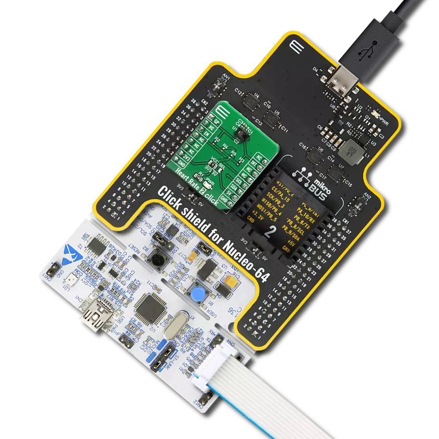
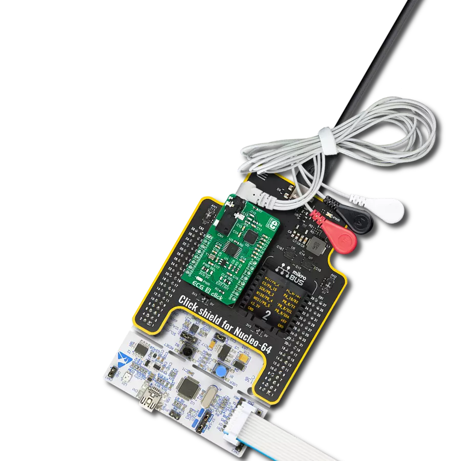
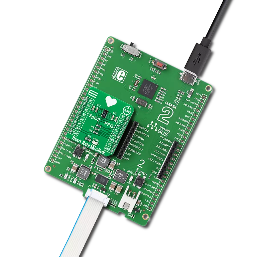
Heart Rate 3 Click
Dev. board
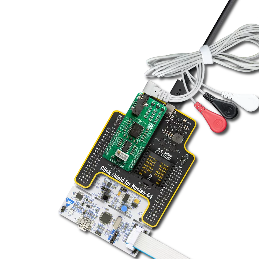
Nucleo 64 with STM32G071RB MCU
Compiler
NECTO Studio
MCU
STM32G071RB
Develop algorithms for pulse oximetry and heart rate readings through the tip of a finger
A
A
Hardware Overview
How does it work?
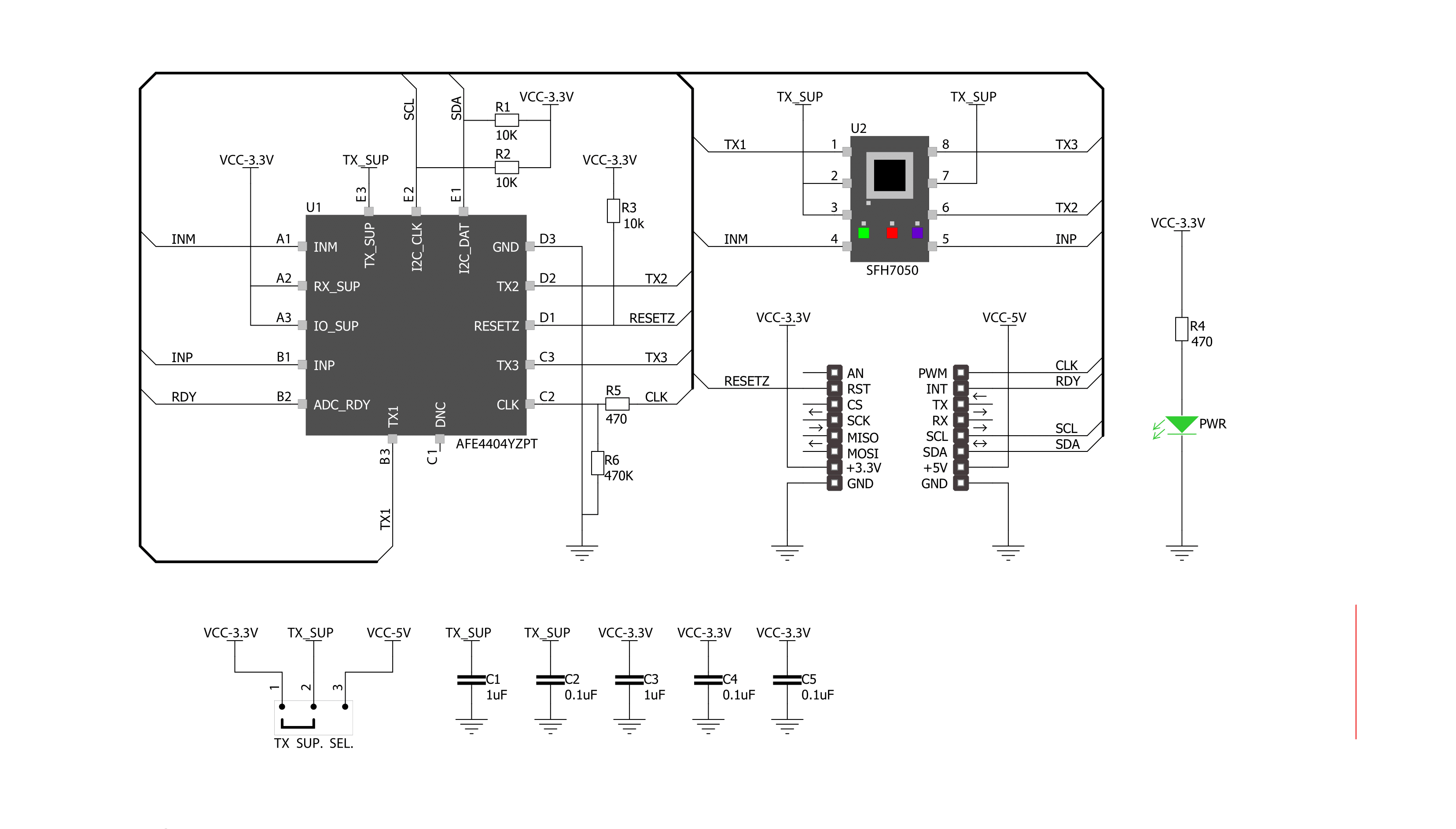
Heart Rate 3 Click is based on the SFH7050, a pulse oximetry and heart rate sensor from ams OSRAM. This multi-chip package consists of three emitters and one detector, with a light barrier to block crosstalk between the LEDs and the detector. These emitters are green, red, and infrared LEDs pointed toward the measuring objects (human skin, finger). The green LED is most commonly used to measure the dilatation of the blood vessels. The red and the infrared LED light are absorbed differently by oxygen-rich and oxygen-poor blood; therefore, the SFH7050 consists of both of them. The peak wavelength differs from each LED, but the half angle is the same for all three LEDs, ± 60°. As a detector, separated by a block barrier, the photodiode detects the intensity of light returned. As mentioned, this Click board™ uses three LEDs and a photodiode to detect the intensity of light returned, and besides them, it also features the AFE4404, an integrated AFE for optical heart-rate monitoring and bio-sensing from Texas Instruments. The AFE4404 includes a 6-bit
programmable LED current for all three LEDs and individual DC offset subtraction DAC at TIA (Transimpedance Amplifier) input for each LED and ambient phase, allowing to increase sensor's accuracy and remove the noise from the signal. There is also a way to average the 24-bit output from the photodiode before sending it to the BPM algorithm for better noise cancellation. To communicate to the host MCU, the Heart Rate 3 Click uses the I2C interface of the AFE4404 over the mikroBUS™ socket. Every time all three LEDs have finished sampling and converting, the interrupt is triggered over the RDY pin, thus saving the host MCU from constantly polling the sensor for data. This pin is set to a high logic level when the PRF (a pulse repetition frequency) cycle ends, allowing four output data register to be read. The PRF can vary between 10 to 1000 samples per second. The clock input can be selected over the CLK pin, as the AFE4404 can be clocked both internally and externally. The input clock can go up to 60MHz, but the internal divider of the IC has to be set so that the clock stays within the range
from 4MHz to 6MHz. When driven by the internal clock, the device runs at 4MHz. By default, the external clock input is selected. The users can choose one of the clock options over the R5 and R6 resistors (R5 for external clock mode and R6 for internal oscillator mode). After the Power-on sequence, the AFE requires a reset. The RST pin of the mikroBUS™ socket allows the AFE to be reset by the host MCU. Pulling this pin to a low logic state for more than 200µs will put the device into the Power Down mode. The AFE can also be reset by setting a bit in the appropriate register via the I2C interface. This Click board™ can only be operated with a 3.3V logic voltage level. The board must perform appropriate logic voltage level conversion before using MCUs with different logic levels. However, the Click board™ comes equipped with a library containing functions and an example code that can be used, as a reference, for further development. Although the Heart Rate 3 Click is a 3.3V logic level only, the onboard LED SUP jumper allows you to set the voltage for driving the SFH7050 LEDs at either 3.3V or 5V.


Features overview
Development board
Nucleo-64 with STM32G071RB MCU offers a cost-effective and adaptable platform for developers to explore new ideas and prototype their designs. This board harnesses the versatility of the STM32 microcontroller, enabling users to select the optimal balance of performance and power consumption for their projects. It accommodates the STM32 microcontroller in the LQFP64 package and includes essential components such as a user LED, which doubles as an ARDUINO® signal, alongside user and reset push-buttons, and a 32.768kHz crystal oscillator for precise timing operations. Designed with expansion and flexibility in mind, the Nucleo-64 board features an ARDUINO® Uno V3 expansion connector and ST morpho extension pin
headers, granting complete access to the STM32's I/Os for comprehensive project integration. Power supply options are adaptable, supporting ST-LINK USB VBUS or external power sources, ensuring adaptability in various development environments. The board also has an on-board ST-LINK debugger/programmer with USB re-enumeration capability, simplifying the programming and debugging process. Moreover, the board is designed to simplify advanced development with its external SMPS for efficient Vcore logic supply, support for USB Device full speed or USB SNK/UFP full speed, and built-in cryptographic features, enhancing both the power efficiency and security of projects. Additional connectivity is
provided through dedicated connectors for external SMPS experimentation, a USB connector for the ST-LINK, and a MIPI® debug connector, expanding the possibilities for hardware interfacing and experimentation. Developers will find extensive support through comprehensive free software libraries and examples, courtesy of the STM32Cube MCU Package. This, combined with compatibility with a wide array of Integrated Development Environments (IDEs), including IAR Embedded Workbench®, MDK-ARM, and STM32CubeIDE, ensures a smooth and efficient development experience, allowing users to fully leverage the capabilities of the Nucleo-64 board in their projects.

Microcontroller Overview
MCU Card / MCU
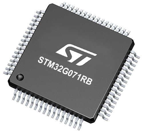
Architecture
ARM Cortex-M0
MCU Memory (KB)
128
Silicon Vendor
STMicroelectronics
Pin count
64
RAM (Bytes)
36864
You complete me!
Accessories
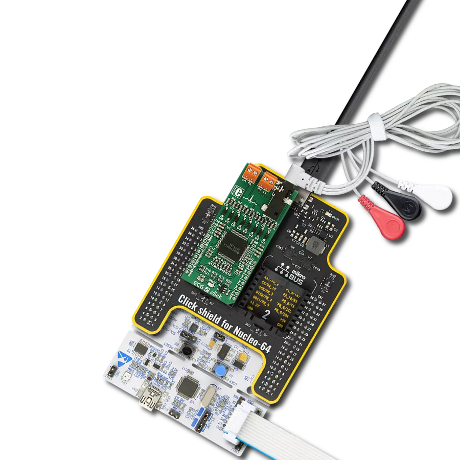
Click Shield for Nucleo-64 comes equipped with two proprietary mikroBUS™ sockets, allowing all the Click board™ devices to be interfaced with the STM32 Nucleo-64 board with no effort. This way, Mikroe allows its users to add any functionality from our ever-growing range of Click boards™, such as WiFi, GSM, GPS, Bluetooth, ZigBee, environmental sensors, LEDs, speech recognition, motor control, movement sensors, and many more. More than 1537 Click boards™, which can be stacked and integrated, are at your disposal. The STM32 Nucleo-64 boards are based on the microcontrollers in 64-pin packages, a 32-bit MCU with an ARM Cortex M4 processor operating at 84MHz, 512Kb Flash, and 96KB SRAM, divided into two regions where the top section represents the ST-Link/V2 debugger and programmer while the bottom section of the board is an actual development board. These boards are controlled and powered conveniently through a USB connection to program and efficiently debug the Nucleo-64 board out of the box, with an additional USB cable connected to the USB mini port on the board. Most of the STM32 microcontroller pins are brought to the IO pins on the left and right edge of the board, which are then connected to two existing mikroBUS™ sockets. This Click Shield also has several switches that perform functions such as selecting the logic levels of analog signals on mikroBUS™ sockets and selecting logic voltage levels of the mikroBUS™ sockets themselves. Besides, the user is offered the possibility of using any Click board™ with the help of existing bidirectional level-shifting voltage translators, regardless of whether the Click board™ operates at a 3.3V or 5V logic voltage level. Once you connect the STM32 Nucleo-64 board with our Click Shield for Nucleo-64, you can access hundreds of Click boards™, working with 3.3V or 5V logic voltage levels.

Used MCU Pins
mikroBUS™ mapper
Take a closer look
Click board™ Schematic
Step by step
Project assembly
Start by selecting your development board and Click board™. Begin with the Nucleo 64 with STM32G071RB MCU as your development board.


Software Support
Library Description
This library contains API for Heart Rate 3 Click driver.
Key functions:
heartrate3_check_data_ready- Function is used to check data ready flagheartrate3_write_data- Function is used to write 32-bit data into registerheartrate3_read_24bit- Function is used to read 24-bit value from register
Open Source
Code example
The complete application code and a ready-to-use project are available through the NECTO Studio Package Manager for direct installation in the NECTO Studio. The application code can also be found on the MIKROE GitHub account.
/*!
 * \file
 * \brief HeartRate3 Click example
 *
 * # Description
 * The demo application shows reflected red, green and ir values.
 *
 * The demo application is composed of two sections :
 *
 * ## Application Init
 * Initalizes Click driver, resets the device, applies default settings
 * and makes an initial log.
 *
 * ## Application Task
 * This example demonstrates the use of Heart rate 3 board. It is set in default
 * mode, and reads reflected red, green and ir values and displays the results
 * on USART terminal.
 *
 * @note
 * We recommend using the SerialPlot tool for data visualizing.
 *
 * \author Jovan Stajkovic
 *
 */
// ------------------------------------------------------------------- INCLUDES

#include "board.h"
#include "log.h"
#include "heartrate3.h"

// ------------------------------------------------------------------ VARIABLES

static heartrate3_t heartrate3;
static log_t logger;

static uint32_t led_2;
static uint32_t aled_2;
static uint32_t led_1;
static uint32_t aled_1;
static uint32_t led_2_aled_2;
static uint32_t led_1_aled_1;

// ------------------------------------------------------ APPLICATION FUNCTIONS

void application_init ( void )
{
    log_cfg_t log_cfg;
    heartrate3_cfg_t heartrate3_cfg;

    /**
     * Logger initialization.
     * Default baud rate: 115200
     * Default log level: LOG_LEVEL_DEBUG
     * @note If USB_UART_RX and USB_UART_TX
     * are defined as HAL_PIN_NC, you will
     * need to define them manually for log to work.
     * See @b LOG_MAP_USB_UART macro definition for detailed explanation.
     */
    LOG_MAP_USB_UART( log_cfg );
    log_init( &logger, &log_cfg );
    log_info( &logger, "---- Application Init ----" );

    //  Click initialization.
    heartrate3_cfg_setup( &heartrate3_cfg );
    HEARTRATE3_MAP_MIKROBUS( heartrate3_cfg, MIKROBUS_1 );
    if ( I2C_MASTER_ERROR == heartrate3_init( &heartrate3, &heartrate3_cfg ) )
    {
        log_error( &logger, " Communication init." );
        for ( ; ; );
    }

    log_printf( &logger, "----------------------\r\n" );
    log_printf( &logger, "  Heart rate 3 Click  \r\n" );
    log_printf( &logger, "----------------------\r\n" );

    if ( HEARTRATE3_ERROR == heartrate3_default_cfg ( &heartrate3 ) )
    {
        log_error( &logger, " Default configuration." );
        for ( ; ; );
    }

    log_printf( &logger, "     Initialised!     \r\n" );
    log_printf( &logger, "----------------------\r\n" );
    log_info( &logger, " Application Task " );
    Delay_ms ( 100 );
}

void application_task ( void )
{
    err_t error_flag = HEARTRATE3_OK;
    if ( heartrate3_check_data_ready ( &heartrate3 ) )
    {
        error_flag |= heartrate3_read_24bit( &heartrate3, HEARTRATE3_REG_LED2VAL, &led_2 );
        error_flag |= heartrate3_read_24bit( &heartrate3, HEARTRATE3_REG_ALED2VAL, &aled_2 );
        error_flag |= heartrate3_read_24bit( &heartrate3, HEARTRATE3_REG_LED1VAL, &led_1 );
        error_flag |= heartrate3_read_24bit( &heartrate3, HEARTRATE3_REG_ALED1VAL, &aled_1 );
        error_flag |= heartrate3_read_24bit( &heartrate3, HEARTRATE3_REG_LED2_ALED2VAL, &led_2_aled_2 );
        error_flag |= heartrate3_read_24bit( &heartrate3, HEARTRATE3_REG_LED1_ALED1VAL, &led_1_aled_1 );
        if ( HEARTRATE3_OK == error_flag )
        {
            log_printf( &logger, "%lu;%lu;%lu;%lu;%lu;%lu;\r\n",
                        led_2, aled_2, led_1, aled_1, led_2_aled_2, led_1_aled_1 );
        }
    }
}

int main ( void )
{
    /* Do not remove this line or clock might not be set correctly. */
    #ifdef PREINIT_SUPPORTED
    preinit();
    #endif

    application_init( );

    for ( ; ; )
    {
        application_task( );
    }

    return 0;
}


// ------------------------------------------------------------------------ END
Additional Support
Resources
Category:Biometrics