Stay on top of heartbeats with SFH 7072 and STM32F031K6
Hear the rhythm of life

Published Oct 01, 2024
Click board™
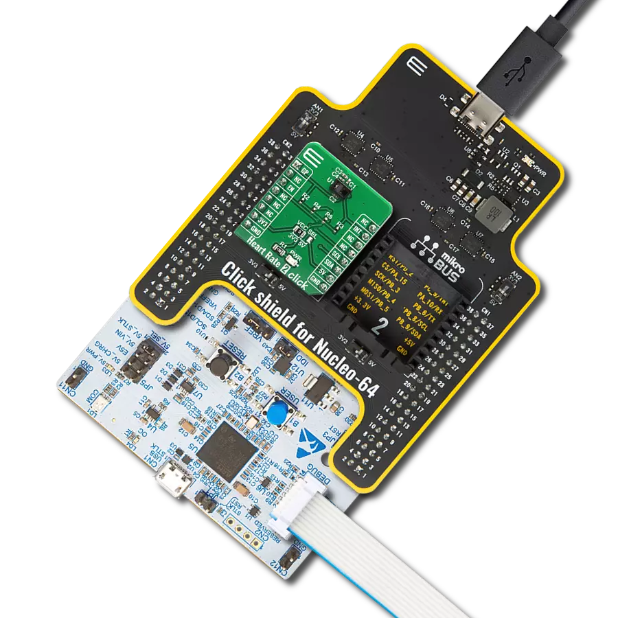
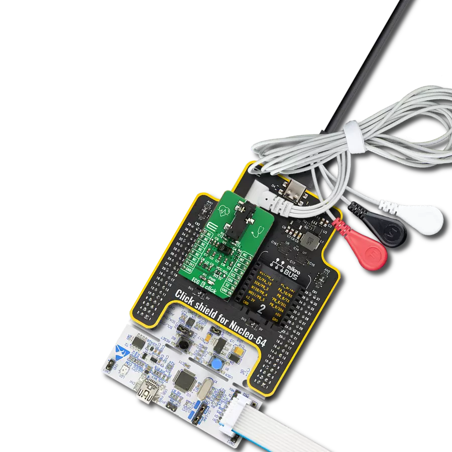
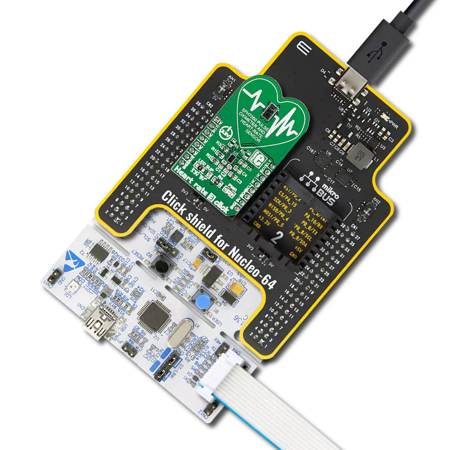
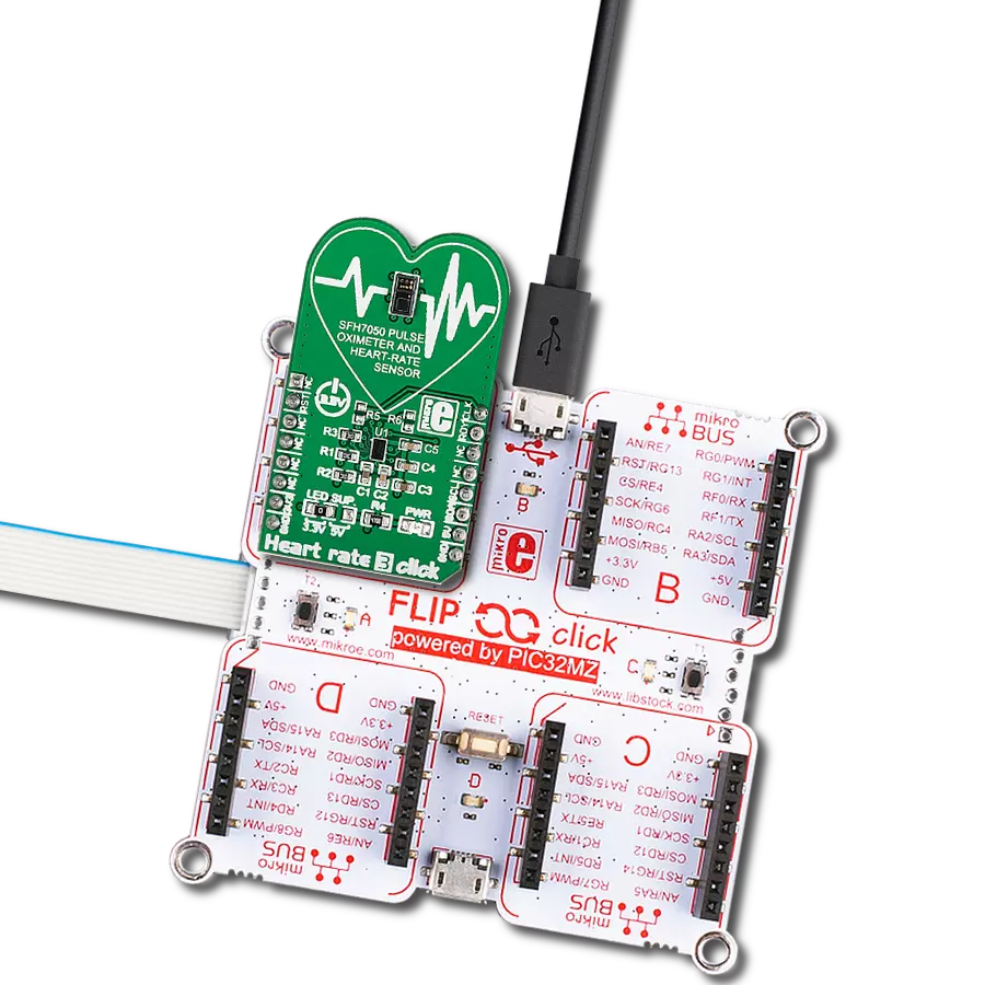
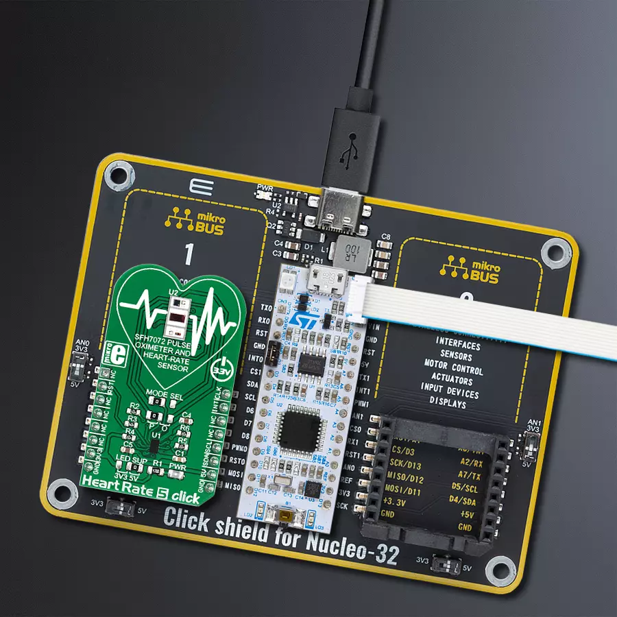
Heart Rate 5 Click
Dev. board
Nucleo 32 with STM32F031K6 MCU
Compiler
NECTO Studio
MCU
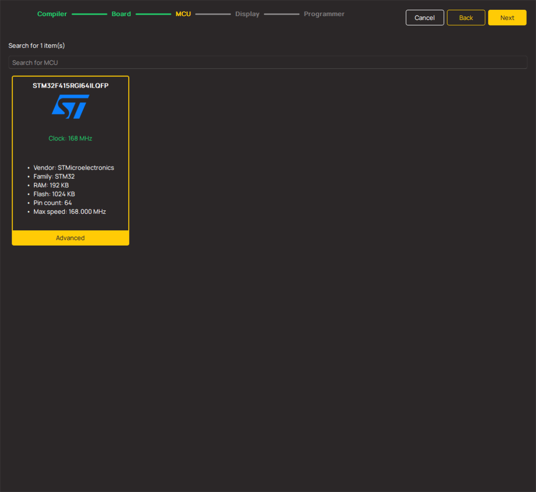
STM32F031K6
Our heart rate monitor aims to empower individuals to take control of their cardiovascular health through accurate and timely heart rate measurements, enabling better self-management
A
A
Hardware Overview
How does it work?
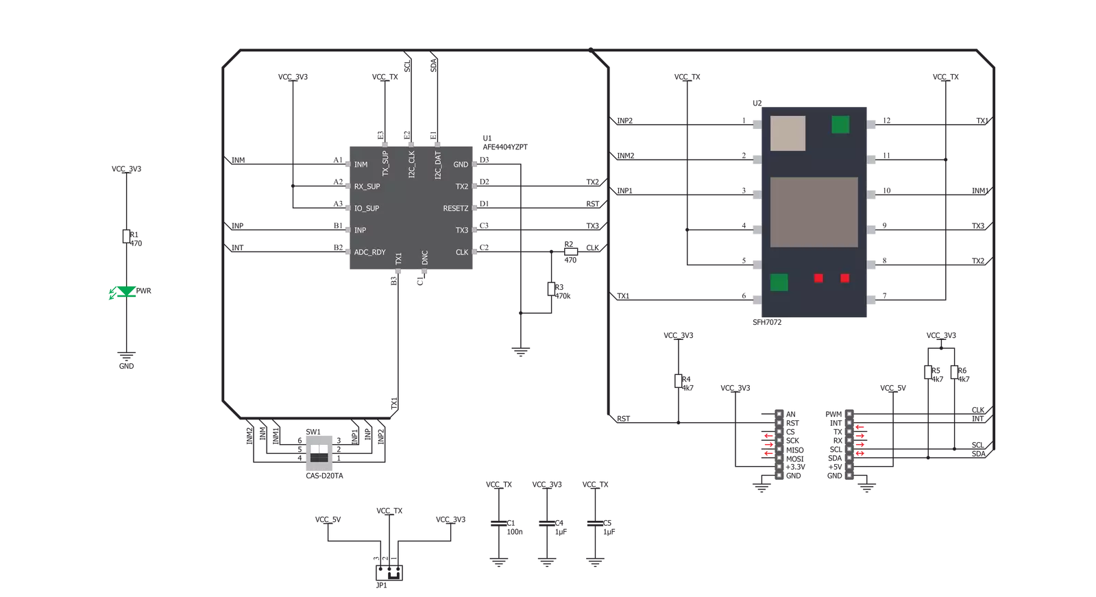
Heart Rate 5 Click consists of an analog front end and the optical front end. The main task of the analog front-end IC is to drive LEDs and condition the signal received by the photodiode (PD) by eliminating the background noise and ambient light influence on the measurement. Besides that, it also provides conversion of the measurement into digital information, which the MCU can use. For the conversion to be accurate, the analog front-end device must not introduce any artifacts into the readings. Heart Rate 5 click employs AFE4404, an integrated analog front-end (AFE) device used for optical heart-rate monitoring and bio-sensing from Texas Instruments to achieve accurate measurements. This IC supports up to three switching LEDs and a single PD element. The current from the PD element is converted to a linear voltage by means of the integrated trans-impedance amplifier section (TIA) with a programmable gain so that it can be sampled by the AD section, which features a 22-bit ADC converter. The signal chain is kept fully differential throughout the receiver channel to achieve good rejection of common-mode noise and the noise from the power supply. The AFE IC uses the I2C communication, with its pins routed to the corresponding mikroBUS™ I2C pins. As the optical front end, Heart Rate 5 click uses the top-of-the-class integrated BIOFY® SFH 7072 sensor from OSRAM, which features two green LEDs, one red LED, one infrared LED, and two PDs, of which one is a broadband PD used for the HRM, while the other is the IR band cut PD, used for the SpO2 readings. These LEDs are specially designed for the HRM and SpO2 measurement applications, offering a set of calibrated wavelengths for both light-emitting diodes (LED) and photo-sensing
diodes (PD). Since the SF7072 sensor offers more elements than the ALS can support, the choice is made by flipping the onboard SMD switch labeled as MODE SEL: the choice can be made between the broadband PD for the HRM readings and the IR band PD for SnO2 readings. Both poles of the switch SW1 need to stay in the same position (both to the left or both to the right), as they are routed to each end of the respective PD element. The analog front end works with periodically repeated operations (a pulse repetition frequency or PRF). There are four sampling phases per cycle. The four different readings are stored in separate 24-bit output registers. There are also four filters on the TIA output, which allow pulses from the PD to pass through the ADC, isolating the time when the emitting LEDs are ON and switching to the different filters in every sampling phase. The sampling phases are determined by the LED modes: two LED modes or three LED modes. This affects which LEDs are pulsed during the corresponding sampling cycles – LED1 and LED2, or LED 1, LED 2, and LED 3. The AFE4404 IC also incorporates a DAC to cancel the DC offset from the PD. When the TIA gain is set to a high value, it will amplify the DC component of the PD signal. This component needs to be removed from the signal path to allow ADC conversion, so the DAC with the opposite current direction is introduced at the input stage based on the existing DC offset. This allows for higher amplification of the signal from the PD and, thus, more useful AC signal detection sensitivity. The LED drivers allow 6 bits of LED current control for each channel individually. This allows 63 steps between 0 and 50mA. This range can be doubled to 100mA. The LED driver voltage can be set by the onboard SMD jumper,
labeled as the LED SUP. It offers a selection between 3.3V and 5V. The ADC_RDY pin provides an interrupt to the host MCU, saving it from having to poll the sensor for data constantly. This pin is set to a HIGH logic level when the PRF cycle ends,allowing four output data register to be read. The PRF can vary between 10 to 1000 samples per second. This pin is routed to the INT pin of the mikroBUS™. The AFE4404 IC can be clocked both internally and externally. It is advised to drive the Heart Rate 5 Click by the same clock as the host MCU for precise and synchronized measurement. The input clock can go up to 60MHz, but the internal divider of the IC has to be set so that the clock stays within the range from 4MHz to 6MHz. When driven by the internal clock, the device runs at 4MHz. By default, the external clock input is selected. The clock signal can be introduced via the PWM pin of the mikroBUS™. After the power-on, the AFE IC requires a reset. The RESETZ pin of this IC is routed to the RST pin of the mikroBUS™, allowing it to be reset by the host MCU. Pulling this signal to a LOW logic level for about 25 µs to 50 µs will cause a device reset. Pulling this pin for more than 200 µs will put the device into the POWER DOWN mode. The device can also be reset by setting a bit in the appropriate register via the I2C. The onboard pull-up resistor pulls This pin to a HIGH logic level. More information about the registers and how to set them can be found in the AFE4404 IC datasheet. However, included library contains functions that allow easy configuration and use of the Heart Rate 5 click. The included exemplary (demo) application demonstrates its functionality and can be used as a reference for a custom design.


Features overview
Development board
Nucleo 32 with STM32F031K6 MCU board provides an affordable and flexible platform for experimenting with STM32 microcontrollers in 32-pin packages. Featuring Arduino™ Nano connectivity, it allows easy expansion with specialized shields, while being mbed-enabled for seamless integration with online resources. The
board includes an on-board ST-LINK/V2-1 debugger/programmer, supporting USB reenumeration with three interfaces: Virtual Com port, mass storage, and debug port. It offers a flexible power supply through either USB VBUS or an external source. Additionally, it includes three LEDs (LD1 for USB communication, LD2 for power,
and LD3 as a user LED) and a reset push button. The STM32 Nucleo-32 board is supported by various Integrated Development Environments (IDEs) such as IAR™, Keil®, and GCC-based IDEs like AC6 SW4STM32, making it a versatile tool for developers.

Microcontroller Overview
MCU Card / MCU

Architecture
ARM Cortex-M0
MCU Memory (KB)
32
Silicon Vendor
STMicroelectronics
Pin count
32
RAM (Bytes)
4096
You complete me!
Accessories
Click Shield for Nucleo-32 is the perfect way to expand your development board's functionalities with STM32 Nucleo-32 pinout. The Click Shield for Nucleo-32 provides two mikroBUS™ sockets to add any functionality from our ever-growing range of Click boards™. We are fully stocked with everything, from sensors and WiFi transceivers to motor control and audio amplifiers. The Click Shield for Nucleo-32 is compatible with the STM32 Nucleo-32 board, providing an affordable and flexible way for users to try out new ideas and quickly create prototypes with any STM32 microcontrollers, choosing from the various combinations of performance, power consumption, and features. The STM32 Nucleo-32 boards do not require any separate probe as they integrate the ST-LINK/V2-1 debugger/programmer and come with the STM32 comprehensive software HAL library and various packaged software examples. This development platform provides users with an effortless and common way to combine the STM32 Nucleo-32 footprint compatible board with their favorite Click boards™ in their upcoming projects.

Used MCU Pins
mikroBUS™ mapper
Take a closer look
Click board™ Schematic
Step by step
Project assembly

Start by selecting your development board and Click board™. Begin with the Nucleo 32 with STM32F031K6 MCU as your development board.


Track your results in real time
Application Output
1. Application Output - In Debug mode, the 'Application Output' window enables real-time data monitoring, offering direct insight into execution results. Ensure proper data display by configuring the environment correctly using the provided tutorial.

2. UART Terminal - Use the UART Terminal to monitor data transmission via a USB to UART converter, allowing direct communication between the Click board™ and your development system. Configure the baud rate and other serial settings according to your project's requirements to ensure proper functionality. For step-by-step setup instructions, refer to the provided tutorial.

3. Plot Output - The Plot feature offers a powerful way to visualize real-time sensor data, enabling trend analysis, debugging, and comparison of multiple data points. To set it up correctly, follow the provided tutorial, which includes a step-by-step example of using the Plot feature to display Click board™ readings. To use the Plot feature in your code, use the function: plot(*insert_graph_name*, variable_name);. This is a general format, and it is up to the user to replace 'insert_graph_name' with the actual graph name and 'variable_name' with the parameter to be displayed.

Software Support
Library Description
This library contains API for Heart rate 5 Click driver.
Key functions:
heartrate5_write_reg- Heart Rate 5 register write functionheartrate5_read_reg- Heart Rate 5 register reading functionheartrate5_sw_reset- Heart Rate 5 software reset function
Open Source
Code example
The complete application code and a ready-to-use project are available through the NECTO Studio Package Manager for direct installation in the NECTO Studio. The application code can also be found on the MIKROE GitHub account.
/*!
 * @file main.c
 * @brief HeartRate5 Click example
 *
 * # Description
 * This example showcases ability for device to read Heart Rate 5 Click Board
 *
 * The demo application is composed of two sections :
 *
 * ## Application Init
 * Configures the micro controller for communication and initializes the Click board.
 *
 * ## Application Task
 * This section shows how the data is processed and sent to the MikroPlot application.
 *
 * @note For testing this example application SerialPlot was used.
 * There you can see heart rate graphicly shown.
 *
 * @author Stefan Ilic
 *
 */

#include "board.h"
#include "log.h"
#include "heartrate5.h"

static heartrate5_t heartrate5;
static log_t logger;
static uint32_t sensor_value;
static uint32_t time = 0;

void application_init ( void )
{
    log_cfg_t log_cfg;  /**< Logger config object. */
    heartrate5_cfg_t heartrate5_cfg;  /**< Click config object. */

    /**
     * Logger initialization.
     * Default baud rate: 115200
     * Default log level: LOG_LEVEL_DEBUG
     * @note If USB_UART_RX and USB_UART_TX
     * are defined as HAL_PIN_NC, you will
     * need to define them manually for log to work.
     * See @b LOG_MAP_USB_UART macro definition for detailed explanation.
     */
    LOG_MAP_USB_UART( log_cfg );
    log_init( &logger, &log_cfg );
    log_info( &logger, " Application Init " );

    // Click initialization.
    heartrate5_cfg_setup( &heartrate5_cfg );
    HEARTRATE5_MAP_MIKROBUS( heartrate5_cfg, MIKROBUS_1 );
    if ( I2C_MASTER_ERROR == heartrate5_init( &heartrate5, &heartrate5_cfg ) )
    {
        log_error( &logger, " Communication init." );
        for ( ; ; );
    }

    if ( HEARTRATE5_ERROR == heartrate5_default_cfg ( &heartrate5 ) )
    {
        log_error( &logger, " Default configuration." );
        for ( ; ; );
    }

    log_info( &logger, " Application Task " );
}

void application_task ( void )
{
    if( heartrate5_get_led2_aled2_val( &heartrate5 ) < 10 )
    {
        sensor_value = heartrate5_get_aled1_val( &heartrate5 );
        log_printf( &logger, "%lu,%lu \r\n", sensor_value, time );
        time += 10;
        Delay_ms ( 10 );
    }
}

int main ( void )
{
    /* Do not remove this line or clock might not be set correctly. */
    #ifdef PREINIT_SUPPORTED
    preinit();
    #endif

    application_init( );

    for ( ; ; )
    {
        application_task( );
    }

    return 0;
}

// ------------------------------------------------------------------------ END
Additional Support
Resources
Category:Biometrics