Seamlessly transform varying frequencies into precise voltage signals with TC9400 and STM32G071RB
Frequency-to-Voltage: Unveiling the magic of signal transformation!

Published Oct 08, 2024
Click board™
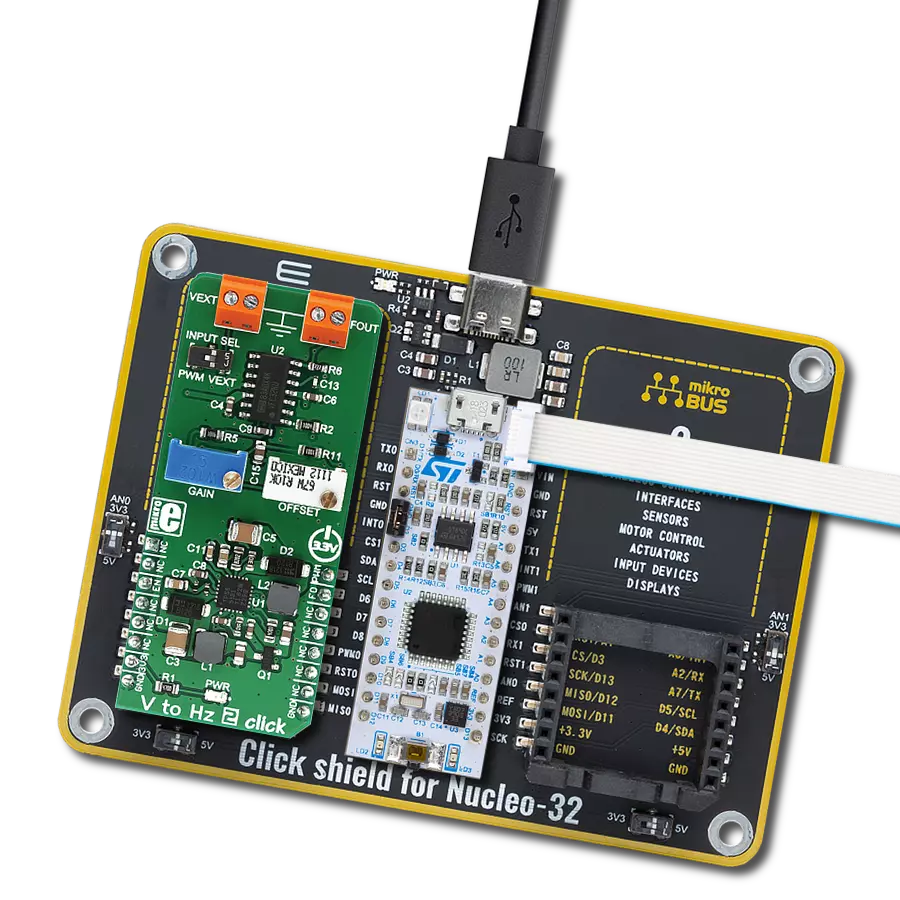
Hz To V Click
Dev. board
Nucleo 64 with STM32G071RB MCU
Compiler
NECTO Studio
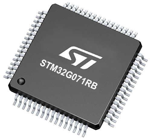
MCU
STM32G071RB
Navigate the world of signal analysis with confidence using our frequency-to-voltage solution, offering unparalleled precision in capturing and converting frequency data into voltage signals
A
A
Hardware Overview
How does it work?
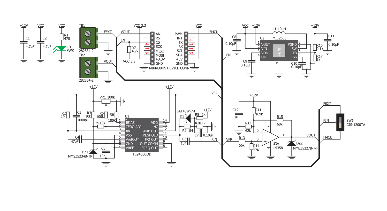
Hz to V Click is based on the TC9400, a voltage-to-frequency and frequency-to-voltage converter from Microchip. It accepts a signal with the frequency within a range between 1kHz and 10kHz on the input and generates DC voltage with the level corresponding to the input frequency, ranging from 0.33V to 3.3V, with a highly linear response. This signal is further passed through the operational amplifier, in order to scale it down to a level acceptable by the MCU. The input signal can be applied either to the PWM pin of the mikroBUS™ or the external input terminal. The input source can be selected with the onboard switch, labeled as INPUT SEL. When Hz to V click is operated for the first time, it needs to be calibrated. The click is equipped with a variable resistor for the offset fine tuning. The following procedure should be followed to calibrate the
device: an input signal with a frequency of 1kHz should be applied to the input. The offset should be adjusted so that a 330mV DC signal appears on the output. Hz to V click is equipped with the input signal terminal (FREQ IN), which is used to connect the signal with a frequency which is in the acceptable range between 1kHz and 10kHz. Besides this signal input terminal, it is possible to select the PWM signal generated by the host MCU as the input, too. INPUT SEL switch can be set so that the PWM pin from the mikroBUS™ is used as the control voltage input. It is recommended that the signal amplitude does not exceed 3.3V. The output terminal (VOLT OUT) is used to output the generated voltage. As already explained, the voltage level depends on the input signal frequency. This generated voltage is also available on the AN pin of the mikroBUS™. The output
signal is passed through the operational amplifier (OPAMP) which is used both as the output buffer and a voltage adjust stage for the output voltage. A well known general purpose operational amplifier LM318 from Texas Instruments is used for this purpose. To provide 12V for the TC9400 and the LM318 OPAMP, Hz to V click employs a boost converter built around the MIC2606, a boost regulator from Microchip, which works at 2MHz. This IC provides 12V for supplying the TC9400 out of 5V routed from the mikroBUS™ socket. The EN pin of the boost regulator is routed to the mikroBUS™ CS pin and it is used to enable power output from the boost regulator, effectively enabling the TC9400 itself. The EN pin is pulled to a HIGH logic level (3.3V) by the onboard resistor.

Features overview
Development board
Nucleo-64 with STM32G071RB MCU offers a cost-effective and adaptable platform for developers to explore new ideas and prototype their designs. This board harnesses the versatility of the STM32 microcontroller, enabling users to select the optimal balance of performance and power consumption for their projects. It accommodates the STM32 microcontroller in the LQFP64 package and includes essential components such as a user LED, which doubles as an ARDUINO® signal, alongside user and reset push-buttons, and a 32.768kHz crystal oscillator for precise timing operations. Designed with expansion and flexibility in mind, the Nucleo-64 board features an ARDUINO® Uno V3 expansion connector and ST morpho extension pin
headers, granting complete access to the STM32's I/Os for comprehensive project integration. Power supply options are adaptable, supporting ST-LINK USB VBUS or external power sources, ensuring adaptability in various development environments. The board also has an on-board ST-LINK debugger/programmer with USB re-enumeration capability, simplifying the programming and debugging process. Moreover, the board is designed to simplify advanced development with its external SMPS for efficient Vcore logic supply, support for USB Device full speed or USB SNK/UFP full speed, and built-in cryptographic features, enhancing both the power efficiency and security of projects. Additional connectivity is
provided through dedicated connectors for external SMPS experimentation, a USB connector for the ST-LINK, and a MIPI® debug connector, expanding the possibilities for hardware interfacing and experimentation. Developers will find extensive support through comprehensive free software libraries and examples, courtesy of the STM32Cube MCU Package. This, combined with compatibility with a wide array of Integrated Development Environments (IDEs), including IAR Embedded Workbench®, MDK-ARM, and STM32CubeIDE, ensures a smooth and efficient development experience, allowing users to fully leverage the capabilities of the Nucleo-64 board in their projects.

Microcontroller Overview
MCU Card / MCU
Architecture
ARM Cortex-M0
MCU Memory (KB)
128
Silicon Vendor
STMicroelectronics
Pin count
64
RAM (Bytes)
36864
You complete me!
Accessories
Click Shield for Nucleo-64 comes equipped with two proprietary mikroBUS™ sockets, allowing all the Click board™ devices to be interfaced with the STM32 Nucleo-64 board with no effort. This way, Mikroe allows its users to add any functionality from our ever-growing range of Click boards™, such as WiFi, GSM, GPS, Bluetooth, ZigBee, environmental sensors, LEDs, speech recognition, motor control, movement sensors, and many more. More than 1537 Click boards™, which can be stacked and integrated, are at your disposal. The STM32 Nucleo-64 boards are based on the microcontrollers in 64-pin packages, a 32-bit MCU with an ARM Cortex M4 processor operating at 84MHz, 512Kb Flash, and 96KB SRAM, divided into two regions where the top section represents the ST-Link/V2 debugger and programmer while the bottom section of the board is an actual development board. These boards are controlled and powered conveniently through a USB connection to program and efficiently debug the Nucleo-64 board out of the box, with an additional USB cable connected to the USB mini port on the board. Most of the STM32 microcontroller pins are brought to the IO pins on the left and right edge of the board, which are then connected to two existing mikroBUS™ sockets. This Click Shield also has several switches that perform functions such as selecting the logic levels of analog signals on mikroBUS™ sockets and selecting logic voltage levels of the mikroBUS™ sockets themselves. Besides, the user is offered the possibility of using any Click board™ with the help of existing bidirectional level-shifting voltage translators, regardless of whether the Click board™ operates at a 3.3V or 5V logic voltage level. Once you connect the STM32 Nucleo-64 board with our Click Shield for Nucleo-64, you can access hundreds of Click boards™, working with 3.3V or 5V logic voltage levels.

Used MCU Pins
mikroBUS™ mapper
Take a closer look
Click board™ Schematic
Step by step
Project assembly
Start by selecting your development board and Click board™. Begin with the Nucleo 64 with STM32G071RB MCU as your development board.


Track your results in real time
Application Output
1. Application Output - In Debug mode, the 'Application Output' window enables real-time data monitoring, offering direct insight into execution results. Ensure proper data display by configuring the environment correctly using the provided tutorial.

2. UART Terminal - Use the UART Terminal to monitor data transmission via a USB to UART converter, allowing direct communication between the Click board™ and your development system. Configure the baud rate and other serial settings according to your project's requirements to ensure proper functionality. For step-by-step setup instructions, refer to the provided tutorial.

3. Plot Output - The Plot feature offers a powerful way to visualize real-time sensor data, enabling trend analysis, debugging, and comparison of multiple data points. To set it up correctly, follow the provided tutorial, which includes a step-by-step example of using the Plot feature to display Click board™ readings. To use the Plot feature in your code, use the function: plot(*insert_graph_name*, variable_name);. This is a general format, and it is up to the user to replace 'insert_graph_name' with the actual graph name and 'variable_name' with the parameter to be displayed.

Software Support
Library Description
This library contains API for Hz To V Click driver.
Key functions:
hztov_read_voltage- Read voltage functionhztov_set_input_frequency- Changing the output voltage function.
Open Source
Code example
The complete application code and a ready-to-use project are available through the NECTO Studio Package Manager for direct installation in the NECTO Studio. The application code can also be found on the MIKROE GitHub account.
/*!
 * \file
 * \brief HzToV Click example
 *
 * # Description
 * This example demonstrates the use of Hz to V click board.
 *
 * The demo application is composed of two sections :
 *
 * ## Application Init
 * Initializes the driver and enables the click board.
 *
 * ## Application Task
 * Sets the PWM frequency then reads the voltage from VO pin and logs all data on USB UART.
 *
 * @note
 * In order to set PWM frequency down to 1 kHz, the user will probably need to
 * lower the main MCU clock frequency.
 * The output voltage may vary, depending on the offset potentiometer setting on the click.
 *
 * \author MikroE Team
 *
 */
// ------------------------------------------------------------------- INCLUDES

#include "board.h"
#include "log.h"
#include "hztov.h"

// ------------------------------------------------------------------ VARIABLES

static hztov_t hztov;
static log_t logger;
static float voltage;
static uint16_t fin;

// ------------------------------------------------------ APPLICATION FUNCTIONS

void application_init ( void )
{
    log_cfg_t log_cfg;
    hztov_cfg_t cfg;

    /**
     * Logger initialization.
     * Default baud rate: 115200
     * Default log level: LOG_LEVEL_DEBUG
     * @note If USB_UART_RX and USB_UART_TX
     * are defined as HAL_PIN_NC, you will
     * need to define them manually for log to work.
     * See @b LOG_MAP_USB_UART macro definition for detailed explanation.
     */
    LOG_MAP_USB_UART( log_cfg );
    log_init( &logger, &log_cfg );
    log_info( &logger, "---- Application Init ----" );

    //  Click initialization.

    hztov_cfg_setup( &cfg );
    HZTOV_MAP_MIKROBUS( cfg, MIKROBUS_1 );
    hztov_init( &hztov, &cfg );

    hztov_set_enable ( &hztov, HZTOV_ENABLE );

    fin = HZTOV_MIN_FREQ;

    Delay_ms( 100 );
}

void application_task ( void )
{
    if ( fin > HZTOV_MAX_FREQ )
        fin = HZTOV_MIN_FREQ;
    hztov_set_input_frequency( &hztov, fin );
    Delay_ms( 1000 );
    log_printf( &logger, "Frequency: %u Hz \r\n", fin );
    voltage = 0;
    for ( uint8_t cnt = 0; cnt < 100; cnt++ )
    {
        voltage += hztov_read_voltage( &hztov );
    }
    log_printf( &logger, "Voltage: %.2f V \r\n", voltage / 100.0 );
    log_printf( &logger, "-------------------\r\n" );

    fin += 1000;
    Delay_ms( 2000 );
}

void main ( void )
{
    application_init( );

    for ( ; ; )
    {
        application_task( );
    }
}


// ------------------------------------------------------------------------ END
Additional Support
Resources
Category:Measurements