Create smarter and more interactive digital experiences with ST25DV16K and STM32F091RC
Touch and transform: NFC readers reshaping your digital landscape

Published Feb 26, 2024
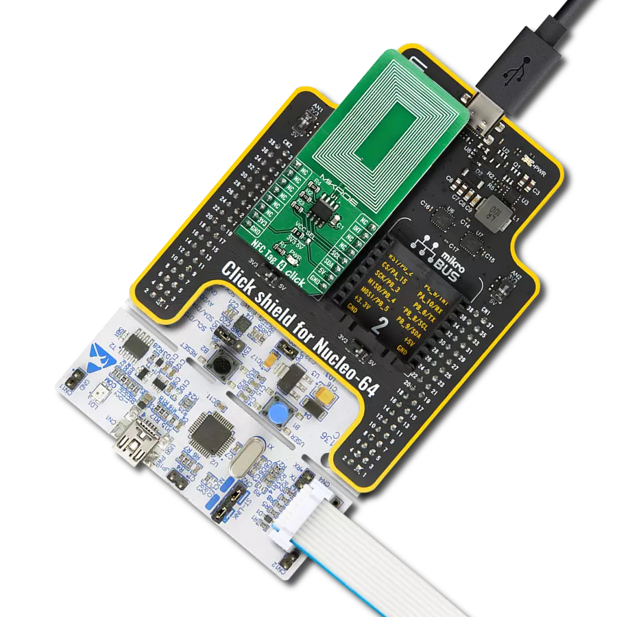
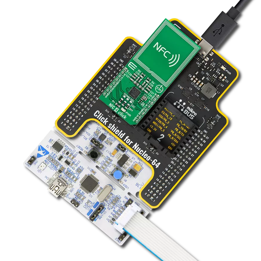
Click board™
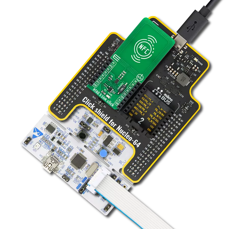
NFC Tag 4 Click
Dev. board
Nucleo-64 with STM32F091RC MCU
Compiler
NECTO Studio
MCU
STM32F091RC
Embrace the NFC experience and see how it extends from simple data sharing to device control, offering a more connected and efficient way of interacting with your digital world
A
A
Hardware Overview
How does it work?
NFC Tag 4 Click is based on the ST25DV16, a compact NFC tag IC from STMicroelectronics. The Click board™ itself has a reasonably small number of components because most of the interface and EEPROM memory circuitry is already integrated on the ST25DV16K IC. The I2C / SMBus compatible serial interface lines, along with the GPO pin, which also works in the open drain configuration, are pulled up by the onboard resistors. The 2-Wire lines are routed to the respective I2C lines of the mikroBUS™ (SCK and SDA), while the GPO pin of the main IC is routed to the INT pin of the mikroBUS™. The ST25DV16K uses the I2C/SMBus compatible communication interface, offering a fast transfer mode (FTM), to achieve a fast link between RF and contact worlds, via a 256 byte buffer called Mailbox. This mailbox dynamic buffer of 256 byte can be filled or emptied via either RF or I2C. There is also the INT pin available, which
indicates incoming event to the contact side, like RF Field changes, RF activity in progress, RF writing completion or Mailbox message availability. The built in energy harvesting element can deliver µW of power when external conditions make it possible. The integrated RF management allows the NFC Tag 4 click to ignore RF requests. All these features can be programmed by setting static and/or dynamic registers of the ST25DV16K. ST25DVxxx can be partially customized using configuration registers located in the E2 system area. More information about all the registers can be found in the ST25DV16K datasheet. However, provided library contains functions that simplify the use of the NFC Tag 4 click. The included application example demonstrates their functionality and it can be used as a reference for custom design. In order to make sure that no external components are required in order to use
it, this Click Board™ contains the integrated trace antenna on the PCB. The antenna coil is correctly tuned and can be used to power and access the device using the ISO/IEC 15693 and ISO 18000-3 mode 1 protocols. Power is transferred to the ST25DV16K by radio frequency at 13.56 MHz via coupling antennas of the NFC Tag 4 click and the NFC Reader being used. The ISO 15693 standard defines the carrier frequency (fC) of the operating field as 13.56 MHz ±7 kHz. This Click board™ can operate with either 3.3V or 5V logic voltage levels selected via the VCC SEL jumper. This way, both 3.3V and 5V capable MCUs can use the communication lines properly. Also, this Click board™ comes equipped with a library containing easy-to-use functions and an example code that can be used as a reference for further development.


Features overview
Development board
Nucleo-64 with STM32F091RC MCU offers a cost-effective and adaptable platform for developers to explore new ideas and prototype their designs. This board harnesses the versatility of the STM32 microcontroller, enabling users to select the optimal balance of performance and power consumption for their projects. It accommodates the STM32 microcontroller in the LQFP64 package and includes essential components such as a user LED, which doubles as an ARDUINO® signal, alongside user and reset push-buttons, and a 32.768kHz crystal oscillator for precise timing operations. Designed with expansion and flexibility in mind, the Nucleo-64 board features an ARDUINO® Uno V3 expansion connector and ST morpho extension pin
headers, granting complete access to the STM32's I/Os for comprehensive project integration. Power supply options are adaptable, supporting ST-LINK USB VBUS or external power sources, ensuring adaptability in various development environments. The board also has an on-board ST-LINK debugger/programmer with USB re-enumeration capability, simplifying the programming and debugging process. Moreover, the board is designed to simplify advanced development with its external SMPS for efficient Vcore logic supply, support for USB Device full speed or USB SNK/UFP full speed, and built-in cryptographic features, enhancing both the power efficiency and security of projects. Additional connectivity is
provided through dedicated connectors for external SMPS experimentation, a USB connector for the ST-LINK, and a MIPI® debug connector, expanding the possibilities for hardware interfacing and experimentation. Developers will find extensive support through comprehensive free software libraries and examples, courtesy of the STM32Cube MCU Package. This, combined with compatibility with a wide array of Integrated Development Environments (IDEs), including IAR Embedded Workbench®, MDK-ARM, and STM32CubeIDE, ensures a smooth and efficient development experience, allowing users to fully leverage the capabilities of the Nucleo-64 board in their projects.

Microcontroller Overview
MCU Card / MCU

Architecture
ARM Cortex-M0
MCU Memory (KB)
256
Silicon Vendor
STMicroelectronics
Pin count
64
RAM (Bytes)
32768
You complete me!
Accessories
Click Shield for Nucleo-64 comes equipped with two proprietary mikroBUS™ sockets, allowing all the Click board™ devices to be interfaced with the STM32 Nucleo-64 board with no effort. This way, Mikroe allows its users to add any functionality from our ever-growing range of Click boards™, such as WiFi, GSM, GPS, Bluetooth, ZigBee, environmental sensors, LEDs, speech recognition, motor control, movement sensors, and many more. More than 1537 Click boards™, which can be stacked and integrated, are at your disposal. The STM32 Nucleo-64 boards are based on the microcontrollers in 64-pin packages, a 32-bit MCU with an ARM Cortex M4 processor operating at 84MHz, 512Kb Flash, and 96KB SRAM, divided into two regions where the top section represents the ST-Link/V2 debugger and programmer while the bottom section of the board is an actual development board. These boards are controlled and powered conveniently through a USB connection to program and efficiently debug the Nucleo-64 board out of the box, with an additional USB cable connected to the USB mini port on the board. Most of the STM32 microcontroller pins are brought to the IO pins on the left and right edge of the board, which are then connected to two existing mikroBUS™ sockets. This Click Shield also has several switches that perform functions such as selecting the logic levels of analog signals on mikroBUS™ sockets and selecting logic voltage levels of the mikroBUS™ sockets themselves. Besides, the user is offered the possibility of using any Click board™ with the help of existing bidirectional level-shifting voltage translators, regardless of whether the Click board™ operates at a 3.3V or 5V logic voltage level. Once you connect the STM32 Nucleo-64 board with our Click Shield for Nucleo-64, you can access hundreds of Click boards™, working with 3.3V or 5V logic voltage levels.

Used MCU Pins
mikroBUS™ mapper
Take a closer look
Click board™ Schematic

Step by step
Project assembly
Start by selecting your development board and Click board™. Begin with the Nucleo-64 with STM32F091RC MCU as your development board.


Track your results in real time
Application Output
1. Application Output - In Debug mode, the 'Application Output' window enables real-time data monitoring, offering direct insight into execution results. Ensure proper data display by configuring the environment correctly using the provided tutorial.

2. UART Terminal - Use the UART Terminal to monitor data transmission via a USB to UART converter, allowing direct communication between the Click board™ and your development system. Configure the baud rate and other serial settings according to your project's requirements to ensure proper functionality. For step-by-step setup instructions, refer to the provided tutorial.

3. Plot Output - The Plot feature offers a powerful way to visualize real-time sensor data, enabling trend analysis, debugging, and comparison of multiple data points. To set it up correctly, follow the provided tutorial, which includes a step-by-step example of using the Plot feature to display Click board™ readings. To use the Plot feature in your code, use the function: plot(*insert_graph_name*, variable_name);. This is a general format, and it is up to the user to replace 'insert_graph_name' with the actual graph name and 'variable_name' with the parameter to be displayed.

Software Support
Library Description
This library contains API for NFC Tag 4 Click driver.
Key functions:
nfctag4_password_present- This function presents password to device in order to open I2C security sessionnfctag4_enable_mailbox- This function enables or disables mailbox functionalitynfctag4_enable_rf- This function enables or disables RF functionality
Open Source
Code example
The complete application code and a ready-to-use project are available through the NECTO Studio Package Manager for direct installation in the NECTO Studio. The application code can also be found on the MIKROE GitHub account.
/*!
 * \file
 * \brief NfcTag4 Click example
 *
* # Description
 * This example showcases how to configure and use the NFC Tag 4 Click. The Click is an NFC tag
 * interface which uses the I2C serial interface and an RF link interface in order to communicate.
 * The example requires the ST25 NFC Tap application which can be downloaded to your phone.
 *
 * The demo application is composed of two sections :
 *
 * ## Application Init
 * This function initializes and configures the logger and Click modules.
 *
 * ## Application Task
 * This function waits for the interrupt signal, after which it expects data transfers. Once
 * some data has been detected it will open a communication channel with the device transmitting
 * it and show the received data in the UART console.
 *
 * \author MikroE Team
 *
 */
// ------------------------------------------------------------------- INCLUDES

#include "board.h"
#include "log.h"
#include "nfctag4.h"

// ------------------------------------------------------------------ VARIABLES

static nfctag4_t nfctag4;
static log_t logger;

static uint8_t aux_buffer[ 258 ];
static uint16_t i;

static uint16_t message_length = 0;
static transfer_info info;

// ------------------------------------------------------- ADDITIONAL FUNCTIONS

void nfctag4_wait_for_int ()
{
    uint16_t timer_counter = 0;
    uint8_t int_pin_flag = 0;
    int_pin_flag = nfctag4_int_get( &nfctag4 );
    while ( ( int_pin_flag == 1 ) && ( timer_counter <= 300 ) )
    {
        Delay_ms ( 1 );
        timer_counter++;
        int_pin_flag = nfctag4_int_get( &nfctag4 );
    }

    if ( timer_counter <= 300 )
    {
        int_pin_flag = nfctag4_int_get( &nfctag4 );
        while ( int_pin_flag == 0 )
        {
            int_pin_flag = nfctag4_int_get( &nfctag4 );
        }
    }

    timer_counter = 0;
}

// ------------------------------------------------------ APPLICATION FUNCTIONS

void application_init ( void )
{
    log_cfg_t log_cfg;
    nfctag4_cfg_t cfg;

    /**
     * Logger initialization.
     * Default baud rate: 115200
     * Default log level: LOG_LEVEL_DEBUG
     * @note If USB_UART_RX and USB_UART_TX
     * are defined as HAL_PIN_NC, you will
     * need to define them manually for log to work.
     * See @b LOG_MAP_USB_UART macro definition for detailed explanation.
     */
    LOG_MAP_USB_UART( log_cfg );
    log_init( &logger, &log_cfg );
    log_info( &logger, "---- Application Init ----" );

    nfctag4_cfg_setup( &cfg );
    NFCTAG4_MAP_MIKROBUS( cfg, MIKROBUS_1 );
    nfctag4_init( &nfctag4, &cfg );

    nfctag4_default_cfg( &nfctag4 );
}

void application_task ( void )
{
    nfctag4_wait_for_int( );

    info.memory_area = NFCTAG4_MEMORY_DYNAMIC;
    info.register_address = NFCTAG4_DYNAMIC_REG_MB_CTRL;
    info.n_registers = 1;
    nfctag4_i2c_get( &nfctag4, &info, aux_buffer );

    if ( ( aux_buffer[ 0 ] & 0x04 ) == ( 0x04 ) )
    {
        nfctag4_wait_for_int( );
        info.memory_area = NFCTAG4_MEMORY_DYNAMIC;
        info.register_address = NFCTAG4_DYNAMIC_REG_MB_LEN;
        info.n_registers = 1;
        nfctag4_i2c_get( &nfctag4, &info, aux_buffer );
        message_length = aux_buffer[ 0 ];
        message_length++;
        nfctag4_wait_for_int( );
        info.memory_area = NFCTAG4_MEMORY_MAILBOX;
        info.register_address = NFCTAG4_MAILBOX_REG_BYTE_0;
        info.n_registers = message_length;
        nfctag4_i2c_get( &nfctag4, &info, aux_buffer );

        log_printf( &logger, "************* MESSAGE ***************\r\n" );
        log_printf( &logger, " ** Message length:  %u Bytes**\r\n", message_length );

        for ( i = 0; i < message_length; i++ )
        {
            log_printf( &logger, " %u : 0x%x\r\n", i, ( uint16_t ) aux_buffer[ i ] );
        }

        log_printf( &logger, "************** END ****************\r\n" );
    }
}

int main ( void )
{
    /* Do not remove this line or clock might not be set correctly. */
    #ifdef PREINIT_SUPPORTED
    preinit();
    #endif

    application_init( );

    for ( ; ; )
    {
        application_task( );
    }

    return 0;
}


// ------------------------------------------------------------------------ END
Additional Support
Resources
Category:RFID/NFC