Empower your electronics with the power of optical isolation based on the LTV-817S and STM32F103RB
Guardian of signals: OptoSentry for total isolation!

Published Oct 08, 2024
Click board™
OPTO 4 Click
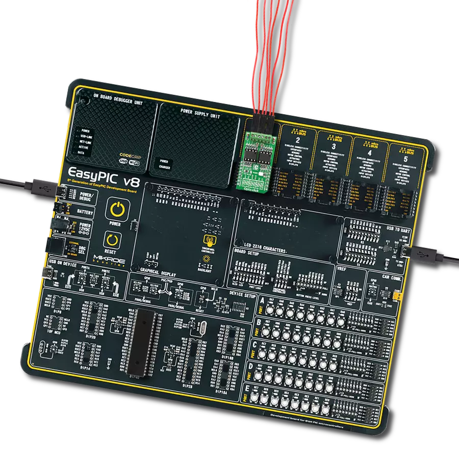
Dev. board
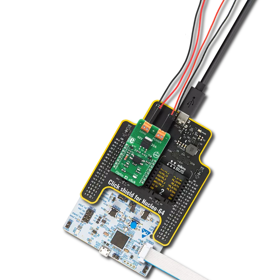
Nucleo 64 with STM32F103RB MCU
Compiler
NECTO Studio
MCU
STM32F103RB
Achieve cleaner and more reliable signal transmission by isolating your circuits from electrical noise and disturbances
A
A
Hardware Overview
How does it work?
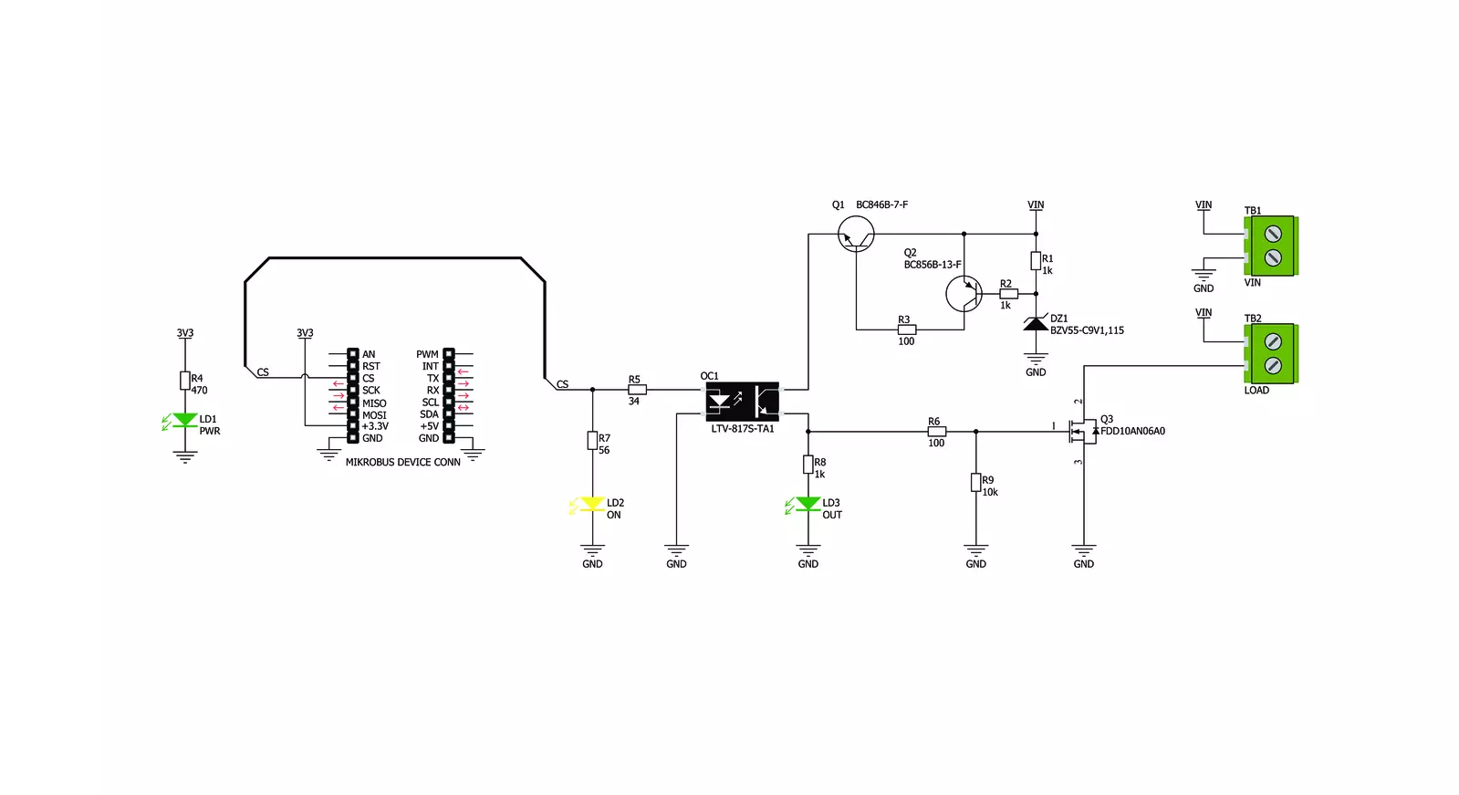
Opto 4 Click is based on the LTV-817S, an optocoupler with a high isolation voltage from ON Semiconductor. This is a single-channel optocoupler which uses the low current provided by the output pin of the microcontroller (MCU) to activate its output stage. Besides an internal biasing LED, the MCU drives an additional external yellow LED, which signalizes that the MCU output is at a HIGH logic level. This led is labeled as ON, and it is used to indicate the state of the optocoupler output stage (conductive or non-conductive). The host MCU uses the CS pin of the mikroBUS™ to drive the input stage of the LTV-817S optocoupler. The working principle of an optocoupler is quite simple: A photo-emitting element - usually an IR LED - is integrated on a die along with the photosensitive element, usually a photosensitive transistor. The LED and the photosensitive transistor are isolated galvanically, but not optically: when the internal LED is powered, it emits light, which biases the base of the photosensitive transistor at the output stage, allowing the current to flow through it. In practice, an optocoupler may be equipped with additional elements such as Schmitt triggers, photo-sensitive Darlington pairs, various configurations of MOSFETs, and more. The output stage of the
optocoupler is used to drive the gate terminal of the FDD10AN06A0, an external power MOSFET, manufactured using the PowerTrench® technology, by ON Semiconductor. This MOSFET allows much more current to flow through the connected load, due to its extremely low ON resistance of about 10 mΩ, typically (10V). This MOSFET is designed to be used in switching circuits and for DC/DC converters, providing a high efficiency for these applications. As such, it has a very low capacitance on its gate terminal, allowing it to be driven with reasonably high-frequency PWM signals. The output stage of the LTV-817S optocoupler is connected to the VIN terminal of the external power supply connector, labeled as POWER. When the output stage of the optocoupler is closed (CS pin of the mikroBUS™ is at a HIGH logic level), it will connect the gate of the power MOSFET to the VIN voltage, thus enabling the power MOSFET. When the output stage of the optocoupler is opened (CS pin is at a LOW logic level), the gate of the MOSFET will be pulled down to the GND, by a 10K resistor, disabling the MOSFET. While enabled, the power MOSFET will be able to conduct the current through an external load, connected to the LOAD terminal. The output stage of the optocoupler also
has a green LED indicator labeled as OUT, which indicates that there is a valid voltage level across the POWER terminal. An undervoltage circuit on the VIN terminal prevents the voltage of the external power supply to drop under 10V. Ideally, the power supply voltage should stay above 12V. It is important for the voltage of the power supply to stay above 10V, since in that case, the ON resistance of the MOSFET is about 10 mΩ, ensuring that no significant heat dissipation will occur as a result of high current through the load. As the voltage of the externally connected power supply drops, it may cause the ON resistance of the power MOSFET to rise enough even before activating the undervoltage circuit (depending on the current through the load), resulting in its damaging. Therefore, the voltage of the external power supply must stay above 10V for this Click board™ to work reliably. The undervoltage protection feature can be useful to switch off the load in the case when the short-circuit condition occurs: the voltage of the power supply during short circuit event may drop, resulting the undervoltage circuit to be activated. However, if a reasonably strong power supply is used, the short-circuit current may be enough to destroy the power MOSFET or the input terminals.


Features overview
Development board
Nucleo-64 with STM32F103RB MCU offers a cost-effective and adaptable platform for developers to explore new ideas and prototype their designs. This board harnesses the versatility of the STM32 microcontroller, enabling users to select the optimal balance of performance and power consumption for their projects. It accommodates the STM32 microcontroller in the LQFP64 package and includes essential components such as a user LED, which doubles as an ARDUINO® signal, alongside user and reset push-buttons, and a 32.768kHz crystal oscillator for precise timing operations. Designed with expansion and flexibility in mind, the Nucleo-64 board features an ARDUINO® Uno V3 expansion connector and ST morpho extension pin
headers, granting complete access to the STM32's I/Os for comprehensive project integration. Power supply options are adaptable, supporting ST-LINK USB VBUS or external power sources, ensuring adaptability in various development environments. The board also has an on-board ST-LINK debugger/programmer with USB re-enumeration capability, simplifying the programming and debugging process. Moreover, the board is designed to simplify advanced development with its external SMPS for efficient Vcore logic supply, support for USB Device full speed or USB SNK/UFP full speed, and built-in cryptographic features, enhancing both the power efficiency and security of projects. Additional connectivity is
provided through dedicated connectors for external SMPS experimentation, a USB connector for the ST-LINK, and a MIPI® debug connector, expanding the possibilities for hardware interfacing and experimentation. Developers will find extensive support through comprehensive free software libraries and examples, courtesy of the STM32Cube MCU Package. This, combined with compatibility with a wide array of Integrated Development Environments (IDEs), including IAR Embedded Workbench®, MDK-ARM, and STM32CubeIDE, ensures a smooth and efficient development experience, allowing users to fully leverage the capabilities of the Nucleo-64 board in their projects.

Microcontroller Overview
MCU Card / MCU
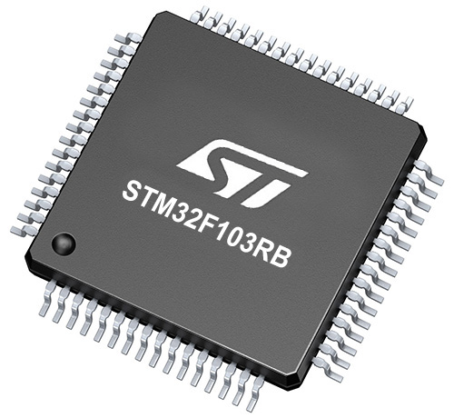
Architecture
ARM Cortex-M3
MCU Memory (KB)
128
Silicon Vendor
STMicroelectronics
Pin count
64
RAM (Bytes)
20480
You complete me!
Accessories
Click Shield for Nucleo-64 comes equipped with two proprietary mikroBUS™ sockets, allowing all the Click board™ devices to be interfaced with the STM32 Nucleo-64 board with no effort. This way, Mikroe allows its users to add any functionality from our ever-growing range of Click boards™, such as WiFi, GSM, GPS, Bluetooth, ZigBee, environmental sensors, LEDs, speech recognition, motor control, movement sensors, and many more. More than 1537 Click boards™, which can be stacked and integrated, are at your disposal. The STM32 Nucleo-64 boards are based on the microcontrollers in 64-pin packages, a 32-bit MCU with an ARM Cortex M4 processor operating at 84MHz, 512Kb Flash, and 96KB SRAM, divided into two regions where the top section represents the ST-Link/V2 debugger and programmer while the bottom section of the board is an actual development board. These boards are controlled and powered conveniently through a USB connection to program and efficiently debug the Nucleo-64 board out of the box, with an additional USB cable connected to the USB mini port on the board. Most of the STM32 microcontroller pins are brought to the IO pins on the left and right edge of the board, which are then connected to two existing mikroBUS™ sockets. This Click Shield also has several switches that perform functions such as selecting the logic levels of analog signals on mikroBUS™ sockets and selecting logic voltage levels of the mikroBUS™ sockets themselves. Besides, the user is offered the possibility of using any Click board™ with the help of existing bidirectional level-shifting voltage translators, regardless of whether the Click board™ operates at a 3.3V or 5V logic voltage level. Once you connect the STM32 Nucleo-64 board with our Click Shield for Nucleo-64, you can access hundreds of Click boards™, working with 3.3V or 5V logic voltage levels.

Used MCU Pins
mikroBUS™ mapper
Take a closer look
Click board™ Schematic
Step by step
Project assembly
Start by selecting your development board and Click board™. Begin with the Nucleo 64 with STM32F103RB MCU as your development board.


Software Support
Library Description
This library contains API for OPTO 4 Click driver.
Key functions:
opto4_output_enable- Function for output enable or disable
Open Source
Code example
The complete application code and a ready-to-use project are available through the NECTO Studio Package Manager for direct installation in the NECTO Studio. The application code can also be found on the MIKROE GitHub account.
/*!
 * \file
 * \brief OPTO 4 Click example
 *
 * # Description
 * This Click sets power on switch enabled and disabled.
 *
 * The demo application is composed of two sections :
 *
 * ## Application Init
 * Initialization driver init.
 *
 * ## Application Task
 * The Output voltage enable and disable every 3 sec.
 *
 * \author MikroE Team
 *
 */
// ------------------------------------------------------------------- INCLUDES

#include "board.h"
#include "log.h"
#include "opto4.h"

// ------------------------------------------------------------------ VARIABLES

static opto4_t opto4;
static log_t logger;

// ------------------------------------------------------ APPLICATION FUNCTIONS

void application_init ( void )
{
    log_cfg_t log_cfg;
    opto4_cfg_t cfg;

    /**
     * Logger initialization.
     * Default baud rate: 115200
     * Default log level: LOG_LEVEL_DEBUG
     * @note If USB_UART_RX and USB_UART_TX
     * are defined as HAL_PIN_NC, you will
     * need to define them manually for log to work.
     * See @b LOG_MAP_USB_UART macro definition for detailed explanation.
     */
    LOG_MAP_USB_UART( log_cfg );
    log_init( &logger, &log_cfg );
    log_info(&logger, "---- Application Init ----");

    //  Click initialization.

    opto4_cfg_setup( &cfg );
    OPTO4_MAP_MIKROBUS( cfg, MIKROBUS_1 );
    opto4_init( &opto4, &cfg );
}

void application_task ( )
{
    opto4_output_enable( &opto4, OPTO4_OUTPUT_ENABLE );
    Delay_ms ( 1000 );
    Delay_ms ( 1000 );
    Delay_ms ( 1000 );
    opto4_output_enable( &opto4, OPTO4_OUTPUT_DISABLE );
    Delay_ms ( 1000 );
    Delay_ms ( 1000 );
    Delay_ms ( 1000 );
}

int main ( void )
{
    /* Do not remove this line or clock might not be set correctly. */
    #ifdef PREINIT_SUPPORTED
    preinit();
    #endif

    application_init( );

    for ( ; ; )
    {
        application_task( );
    }

    return 0;
}


// ------------------------------------------------------------------------ END
Additional Support
Resources
Category:Optocoupler