Harness the power of our captivating random number generator with ADS1115 and STM32F446RE
Random wonders: Numbers beyond predictions!

Published Oct 08, 2024
Click board™
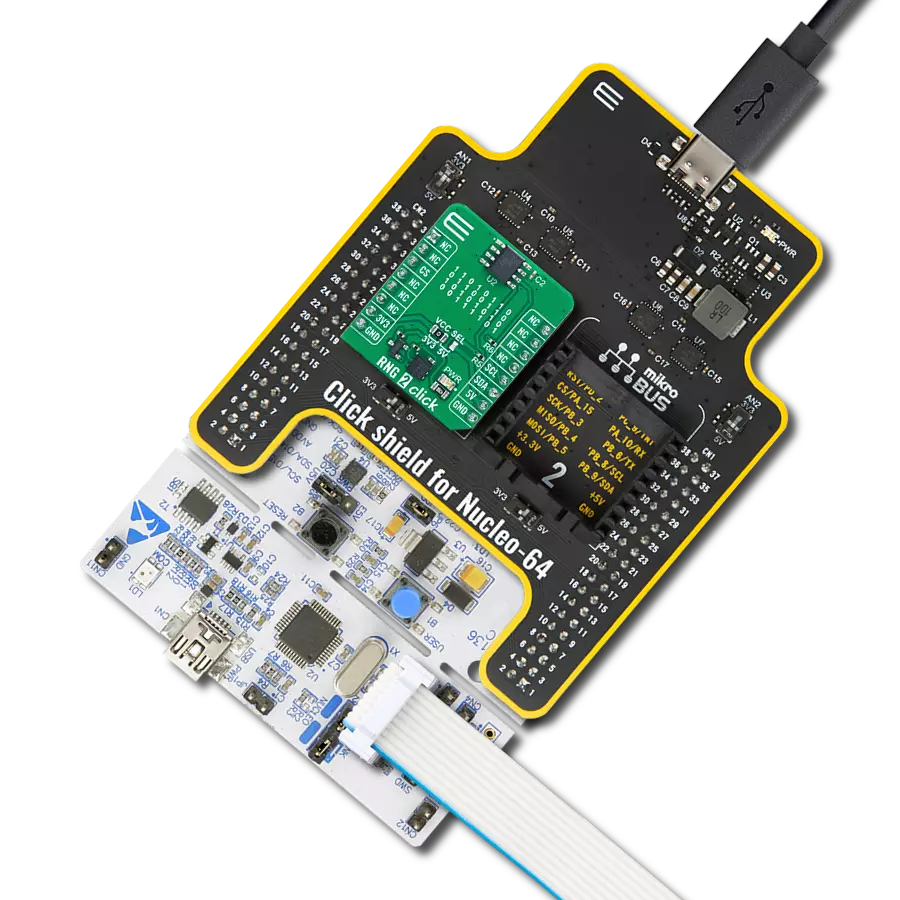
RNG Click
Dev. board
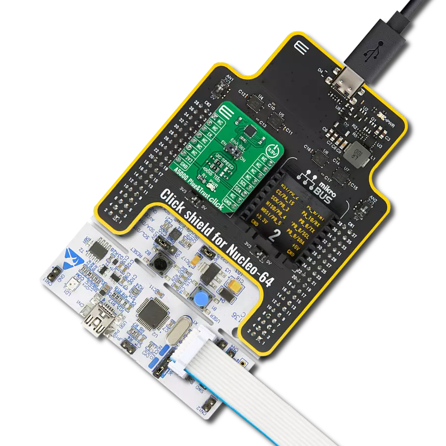
Nucleo 64 with STM32F446RE MCU
Compiler
NECTO Studio
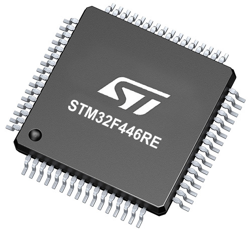
MCU
STM32F446RE
Enhance your decision-making processes by integrating our innovative random number generator into your applications, ensuring selection fairness and eliminating biases
A
A
Hardware Overview
How does it work?
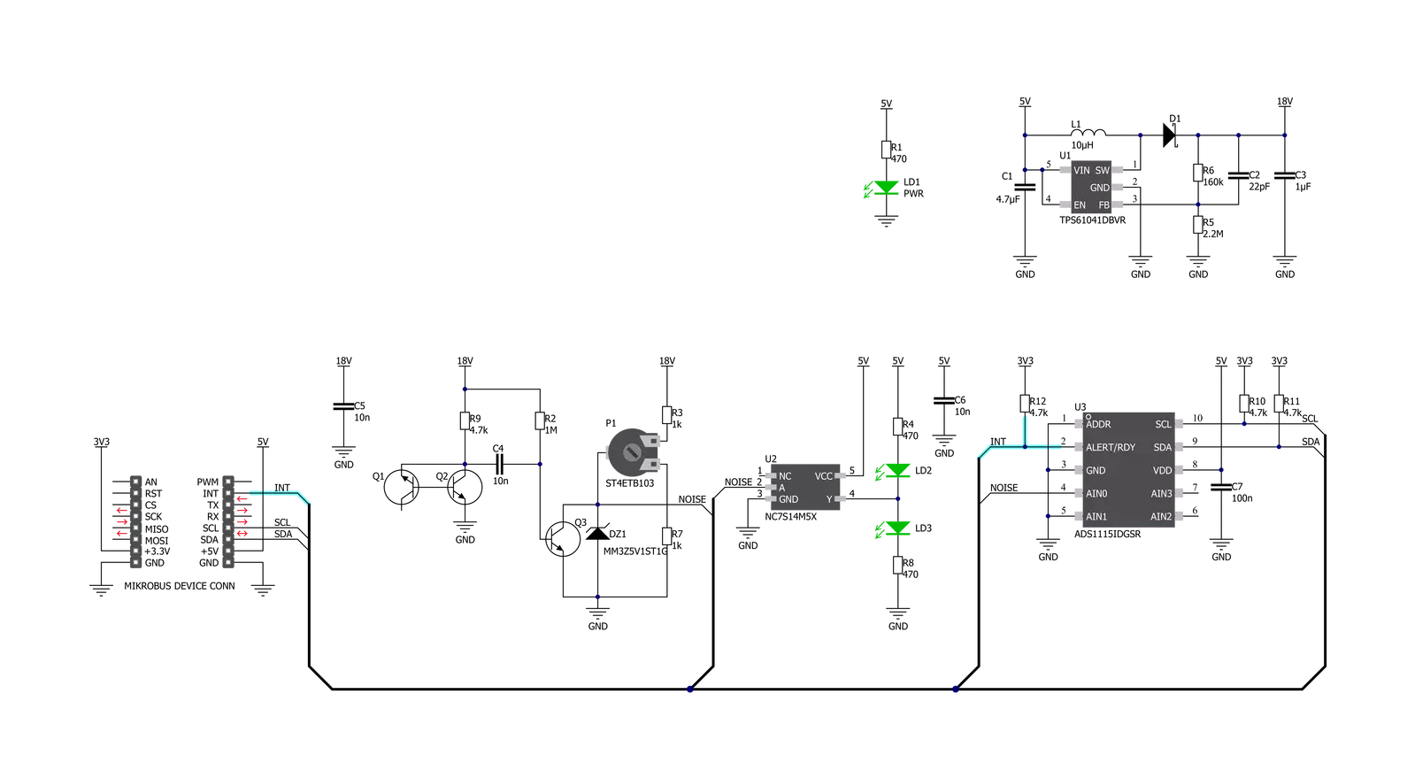
RNG Click is a random number generator (RNG) based on the ADS1115, 16-bit, I2C-compatible, analog-to-digital converter from Texas Instruments that generates a sequence of numbers or symbols that cannot be reasonably predicted better than by a random chance. In computing, a hardware random number generator (HRNG) or true random number generator (TRNG) is a device that generates random numbers from a physical process rather than using an algorithm. Such devices are often based on microscopic phenomena that generate low-level, statistically random "noise" signals, as in this Click board™. That process is, in theory, completely unpredictable, and the theory's assertions of unpredictability are subject to experimental tests. This is in contrast to the paradigm of pseudo-random number generation, which is commonly implemented by the
software. The heart of the RNG click is the avalanche noise generated from an internal diode of the transistor Q1 (BC846B). Avalanche breakdown is a phenomenon that can occur in both insulating and semiconducting materials. It is a form of electric current multiplication that can allow large currents within materials that are otherwise good insulators. The avalanche occurs when the electric field accelerates carriers in the transition region to energies sufficient to create mobile or free electron-hole pairs via collisions with bound electrons. To achieve that, RNG Click also has a boost converter onboard, based on TPS61041 from Texas Instruments, and creates the +18V power supply for the job. The noise signal, created by the transistors Q1 and Q2, is then amplified with Q3, voltage-limited using the Zener diode, and digitalized using the NC7S14M5X inverter. After that, the string of random ones and
zeros is achieved, which is brought to the ADS1115 - 16BIT sigma-delta ADC from Texas Instruments. The potentiometer P1 is used to set the distribution of ones and zeros as near as possible, which is indicated by the LD2 and LD3 LED diodes. The potentiometer P1 should be set to illuminate the LD2 and LD3 diodes equally. That way, when the single-shot measurement is performed using the ADS1115 over the I2C protocol, the true, 16-bit random number is obtained. This Click board™ can be operated only with a 3.3V logic voltage level. The board must perform appropriate logic voltage level conversion before using MCUs with different logic levels. Also, it comes equipped with a library containing functions and an example code that can be used, as a reference, for further development.

Features overview
Development board
Nucleo-64 with STM32F446RE MCU offers a cost-effective and adaptable platform for developers to explore new ideas and prototype their designs. This board harnesses the versatility of the STM32 microcontroller, enabling users to select the optimal balance of performance and power consumption for their projects. It accommodates the STM32 microcontroller in the LQFP64 package and includes essential components such as a user LED, which doubles as an ARDUINO® signal, alongside user and reset push-buttons, and a 32.768kHz crystal oscillator for precise timing operations. Designed with expansion and flexibility in mind, the Nucleo-64 board features an ARDUINO® Uno V3 expansion connector and ST morpho extension pin
headers, granting complete access to the STM32's I/Os for comprehensive project integration. Power supply options are adaptable, supporting ST-LINK USB VBUS or external power sources, ensuring adaptability in various development environments. The board also has an on-board ST-LINK debugger/programmer with USB re-enumeration capability, simplifying the programming and debugging process. Moreover, the board is designed to simplify advanced development with its external SMPS for efficient Vcore logic supply, support for USB Device full speed or USB SNK/UFP full speed, and built-in cryptographic features, enhancing both the power efficiency and security of projects. Additional connectivity is
provided through dedicated connectors for external SMPS experimentation, a USB connector for the ST-LINK, and a MIPI® debug connector, expanding the possibilities for hardware interfacing and experimentation. Developers will find extensive support through comprehensive free software libraries and examples, courtesy of the STM32Cube MCU Package. This, combined with compatibility with a wide array of Integrated Development Environments (IDEs), including IAR Embedded Workbench®, MDK-ARM, and STM32CubeIDE, ensures a smooth and efficient development experience, allowing users to fully leverage the capabilities of the Nucleo-64 board in their projects.

Microcontroller Overview
MCU Card / MCU
Architecture
ARM Cortex-M4
MCU Memory (KB)
512
Silicon Vendor
STMicroelectronics
Pin count
64
RAM (Bytes)
131072
You complete me!
Accessories
Click Shield for Nucleo-64 comes equipped with two proprietary mikroBUS™ sockets, allowing all the Click board™ devices to be interfaced with the STM32 Nucleo-64 board with no effort. This way, Mikroe allows its users to add any functionality from our ever-growing range of Click boards™, such as WiFi, GSM, GPS, Bluetooth, ZigBee, environmental sensors, LEDs, speech recognition, motor control, movement sensors, and many more. More than 1537 Click boards™, which can be stacked and integrated, are at your disposal. The STM32 Nucleo-64 boards are based on the microcontrollers in 64-pin packages, a 32-bit MCU with an ARM Cortex M4 processor operating at 84MHz, 512Kb Flash, and 96KB SRAM, divided into two regions where the top section represents the ST-Link/V2 debugger and programmer while the bottom section of the board is an actual development board. These boards are controlled and powered conveniently through a USB connection to program and efficiently debug the Nucleo-64 board out of the box, with an additional USB cable connected to the USB mini port on the board. Most of the STM32 microcontroller pins are brought to the IO pins on the left and right edge of the board, which are then connected to two existing mikroBUS™ sockets. This Click Shield also has several switches that perform functions such as selecting the logic levels of analog signals on mikroBUS™ sockets and selecting logic voltage levels of the mikroBUS™ sockets themselves. Besides, the user is offered the possibility of using any Click board™ with the help of existing bidirectional level-shifting voltage translators, regardless of whether the Click board™ operates at a 3.3V or 5V logic voltage level. Once you connect the STM32 Nucleo-64 board with our Click Shield for Nucleo-64, you can access hundreds of Click boards™, working with 3.3V or 5V logic voltage levels.

Used MCU Pins
mikroBUS™ mapper
Take a closer look
Click board™ Schematic
Step by step
Project assembly
Start by selecting your development board and Click board™. Begin with the Nucleo 64 with STM32F446RE MCU as your development board.


Software Support
Library Description
This library contains API for RNG Click driver.
Key functions:
rng_get_voltage- This function gets voltage in millivoltsrng_set_config- This function sets configurationrng_set_vref- This function sets desired vref.
Open Source
Code example
The complete application code and a ready-to-use project are available through the NECTO Studio Package Manager for direct installation in the NECTO Studio. The application code can also be found on the MIKROE GitHub account.
/*!
 * \file
 * \brief Rng Click example
 *
 * # Description
 * This Click is a random number generator. The device contain potentiometer which control voltage
 * so it generates a sequence of numbers or symbols that cannot be reasonably predicted better
 * by a random chance. Random number generators have applications in gambling, statistical sampling,
 * computer simulation, cryptography, completely randomized design, and various other areas.
 *
 * The demo application is composed of two sections :
 *
 * ## Application Init
 * Initializes driver, then sets configuration and voltage reference.
 *
 * ## Application Task
 * It reads ADC value from AIN0 channel then converts it to voltage and
 * displays the result on USB UART each second.
 *
 * \author MikroE Team
 *
 */
// ------------------------------------------------------------------- INCLUDES

#include "board.h"
#include "log.h"
#include "rng.h"

// ------------------------------------------------------------------ VARIABLES

static rng_t rng;
static log_t logger;

// ------------------------------------------------------ APPLICATION FUNCTIONS

void application_init ( void )
{
    log_cfg_t log_cfg;
    rng_cfg_t cfg;

    /**
     * Logger initialization.
     * Default baud rate: 115200
     * Default log level: LOG_LEVEL_DEBUG
     * @note If USB_UART_RX and USB_UART_TX
     * are defined as HAL_PIN_NC, you will
     * need to define them manually for log to work.
     * See @b LOG_MAP_USB_UART macro definition for detailed explanation.
     */
    LOG_MAP_USB_UART( log_cfg );
    log_init( &logger, &log_cfg );
    log_info( &logger, "---- Application Init ----" );

    //  Click initialization.

    rng_cfg_setup( &cfg );
    RNG_MAP_MIKROBUS( cfg, MIKROBUS_1 );
    rng_init( &rng, &cfg );

    rng_default_cfg( &rng );
}

void application_task ( void )
{
    float voltage;

    voltage = rng_get_voltage( &rng );

    log_printf( &logger, "Voltage from AIN0: %.2f mV\r\n", voltage );
    log_printf( &logger, "-----------------------\r\n" );
    Delay_ms ( 1000 );
}

int main ( void )
{
    /* Do not remove this line or clock might not be set correctly. */
    #ifdef PREINIT_SUPPORTED
    preinit();
    #endif

    application_init( );

    for ( ; ; )
    {
        application_task( );
    }

    return 0;
}


// ------------------------------------------------------------------------ END
Additional Support
Resources
Category:Encryption