Experience the magic of protocol transformation with SC18IM704 and STM32L073RZ
UART to I2C wizardry: Your communication transformer!

Published Feb 26, 2024
Click board™
UART to I2C Click
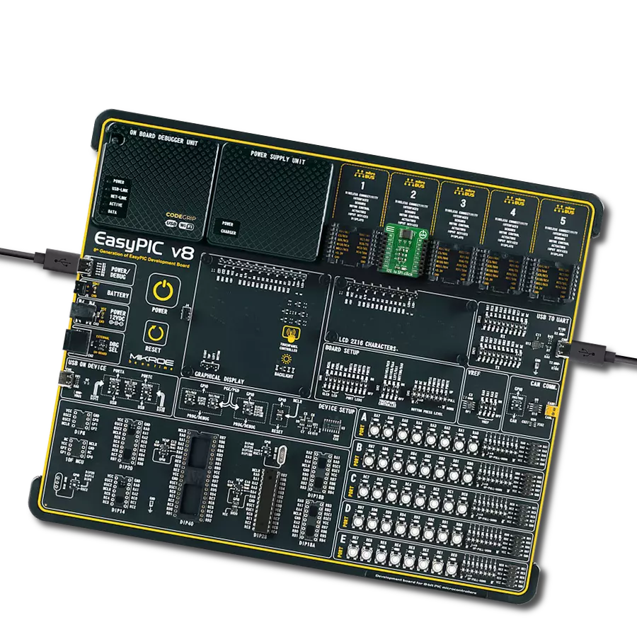
Dev. board
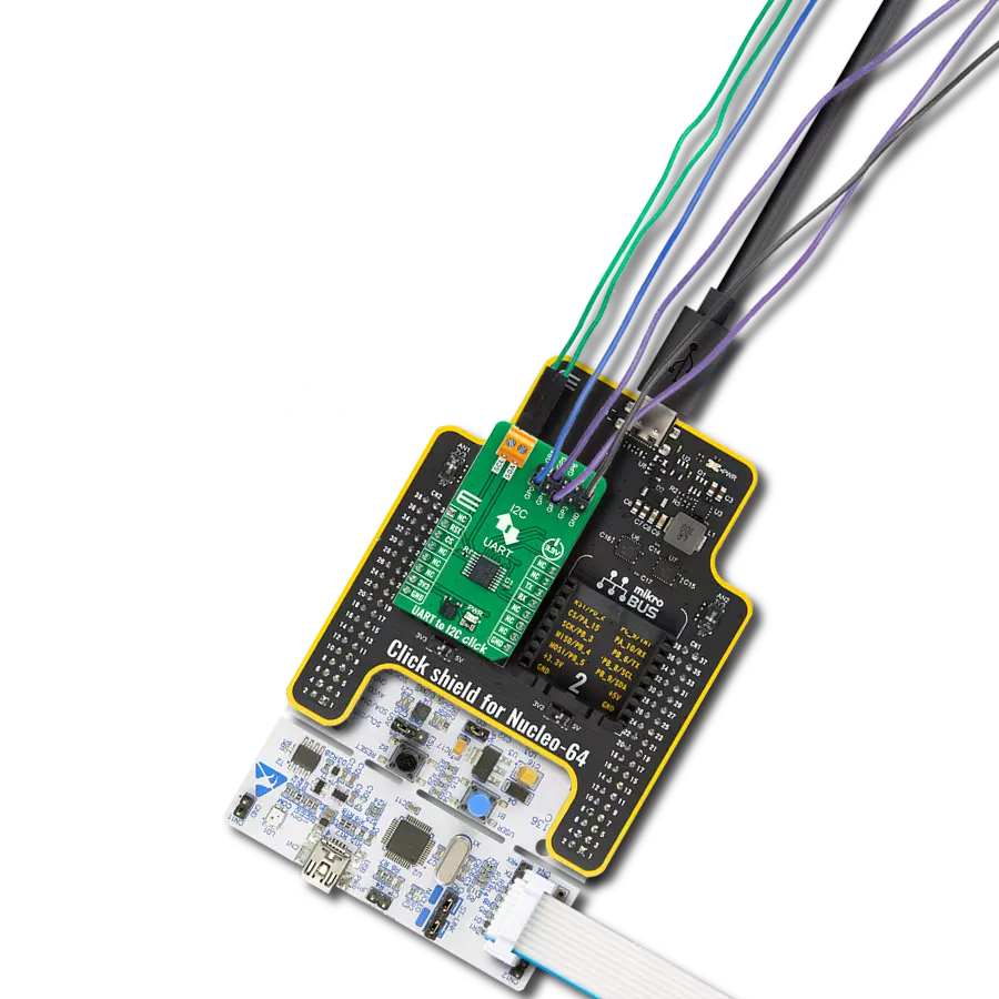
Nucleo-64 with STM32L073RZ MCU
Compiler
NECTO Studio
MCU
STM32L073RZ
Unlock the potential of your UART devices by effortlessly integrating them into I2C networks using our transformation solution, simplifying data exchange and enhancing control
A
A
Hardware Overview
How does it work?
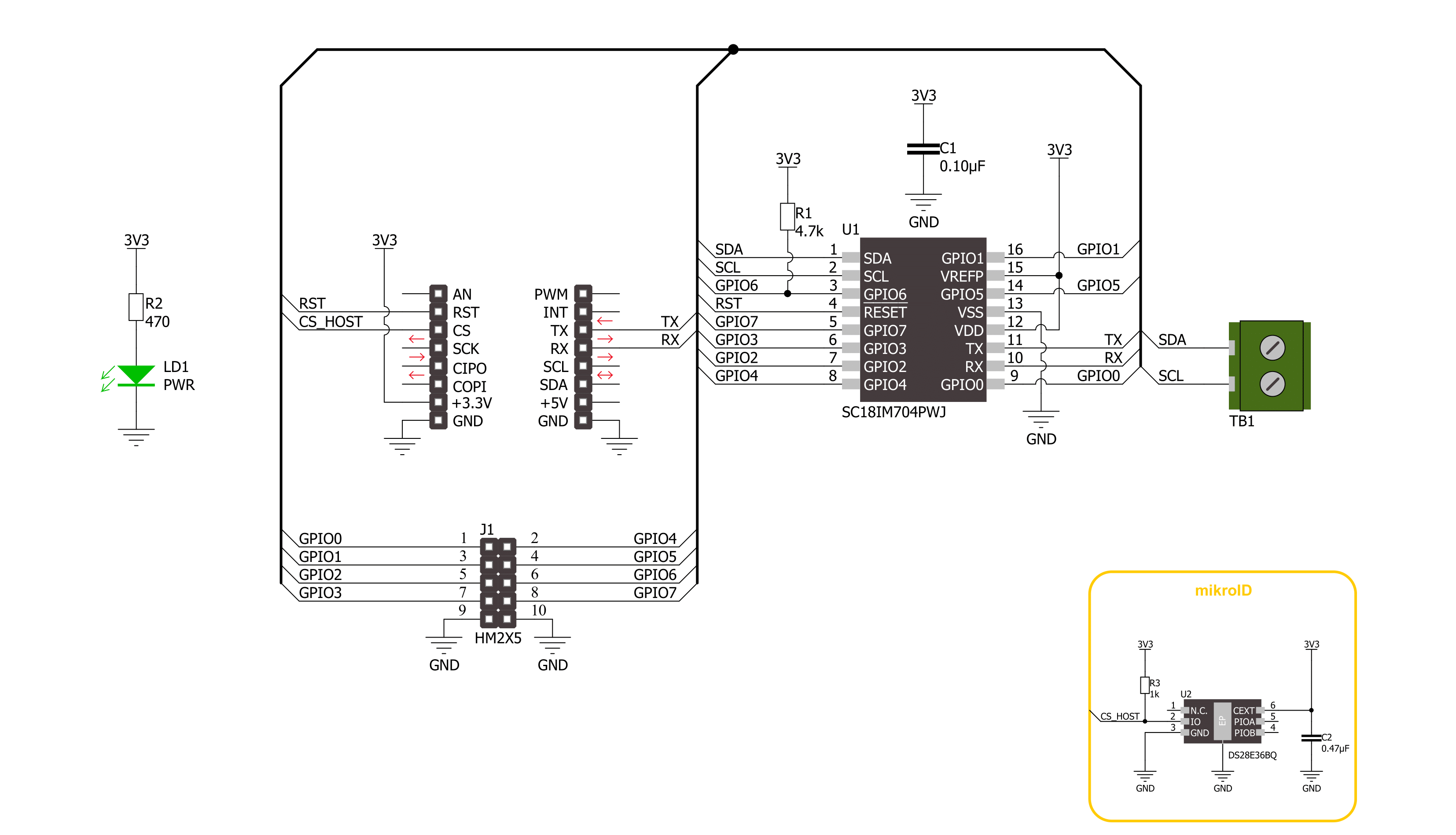
UART to I2C Click is based on the SC18IM704, a bridge between the standard UART port and a serial I2C bus from NXP Semiconductors. The SC18IM704 consists of a full-functional advanced UART interface that communicates with the host MCU through the commonly used RX and TX pins of the mikroBUS™ socket. It is also characterized by a high baud rate of up to 460.8 kbit/s and 256-byte FIFO for the transfer/receive data process. The serial data format is fixed to a one start bit, 8 data bits, and one stop bit. After the reset feature, the baud rate defaults to 9600 bit/s and can be changed through the Baud Rate Generator (BRG) registers. After a Power-Up sequence or already-mentioned hardware reset, achievable through the RST pin of the mikroBUS™ socket, the
SC18IM704 will send two continuous bytes to the host MCU to indicate a Start-Up condition. These two continuous bytes are 0x4F and 0x4B, representing an ‘OK’ state in the ASCII messages protocol. After the correct initial sequence, direct communication is enabled with other I2C-bus devices connected to the populated I2C-bus terminal. The I2C bus uses two wires (SCL and SDA) to transfer information between connected devices, providing a byte-oriented interface that supports data transfers up to 400kHz. The SC18IM704 can also be placed in a software-configurable low-power mode (Power-Down mode). Upon entering the Power-Down state, the UART RX pin is used to exit Deep Power-down mode. The bridge remains in the Deep
Power-down mode as long as the RX pin remains in a high logic state. Any character sent brings the bridge out of Deep Power-down mode but ignores the character. In addition to all these features, the SC18IM704 has several general-purpose I/O pins on the populated header with labeled GP pins. These pins have the option of software setting their function as push-pull, open-drain, or input-only. This Click board™ can be operated only with a 3.3V logic voltage level. The board must perform appropriate logic voltage level conversion before using MCUs with different logic levels. Also, it comes equipped with a library containing functions and an example code that can be used as a reference for further development.


Features overview
Development board
Nucleo-64 with STM32L073RZ MCU offers a cost-effective and adaptable platform for developers to explore new ideas and prototype their designs. This board harnesses the versatility of the STM32 microcontroller, enabling users to select the optimal balance of performance and power consumption for their projects. It accommodates the STM32 microcontroller in the LQFP64 package and includes essential components such as a user LED, which doubles as an ARDUINO® signal, alongside user and reset push-buttons, and a 32.768kHz crystal oscillator for precise timing operations. Designed with expansion and flexibility in mind, the Nucleo-64 board features an ARDUINO® Uno V3 expansion connector and ST morpho extension pin
headers, granting complete access to the STM32's I/Os for comprehensive project integration. Power supply options are adaptable, supporting ST-LINK USB VBUS or external power sources, ensuring adaptability in various development environments. The board also has an on-board ST-LINK debugger/programmer with USB re-enumeration capability, simplifying the programming and debugging process. Moreover, the board is designed to simplify advanced development with its external SMPS for efficient Vcore logic supply, support for USB Device full speed or USB SNK/UFP full speed, and built-in cryptographic features, enhancing both the power efficiency and security of projects. Additional connectivity is
provided through dedicated connectors for external SMPS experimentation, a USB connector for the ST-LINK, and a MIPI® debug connector, expanding the possibilities for hardware interfacing and experimentation. Developers will find extensive support through comprehensive free software libraries and examples, courtesy of the STM32Cube MCU Package. This, combined with compatibility with a wide array of Integrated Development Environments (IDEs), including IAR Embedded Workbench®, MDK-ARM, and STM32CubeIDE, ensures a smooth and efficient development experience, allowing users to fully leverage the capabilities of the Nucleo-64 board in their projects.

Microcontroller Overview
MCU Card / MCU
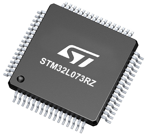
Architecture
ARM Cortex-M0
MCU Memory (KB)
192
Silicon Vendor
STMicroelectronics
Pin count
64
RAM (Bytes)
20480
You complete me!
Accessories
Click Shield for Nucleo-64 comes equipped with two proprietary mikroBUS™ sockets, allowing all the Click board™ devices to be interfaced with the STM32 Nucleo-64 board with no effort. This way, Mikroe allows its users to add any functionality from our ever-growing range of Click boards™, such as WiFi, GSM, GPS, Bluetooth, ZigBee, environmental sensors, LEDs, speech recognition, motor control, movement sensors, and many more. More than 1537 Click boards™, which can be stacked and integrated, are at your disposal. The STM32 Nucleo-64 boards are based on the microcontrollers in 64-pin packages, a 32-bit MCU with an ARM Cortex M4 processor operating at 84MHz, 512Kb Flash, and 96KB SRAM, divided into two regions where the top section represents the ST-Link/V2 debugger and programmer while the bottom section of the board is an actual development board. These boards are controlled and powered conveniently through a USB connection to program and efficiently debug the Nucleo-64 board out of the box, with an additional USB cable connected to the USB mini port on the board. Most of the STM32 microcontroller pins are brought to the IO pins on the left and right edge of the board, which are then connected to two existing mikroBUS™ sockets. This Click Shield also has several switches that perform functions such as selecting the logic levels of analog signals on mikroBUS™ sockets and selecting logic voltage levels of the mikroBUS™ sockets themselves. Besides, the user is offered the possibility of using any Click board™ with the help of existing bidirectional level-shifting voltage translators, regardless of whether the Click board™ operates at a 3.3V or 5V logic voltage level. Once you connect the STM32 Nucleo-64 board with our Click Shield for Nucleo-64, you can access hundreds of Click boards™, working with 3.3V or 5V logic voltage levels.

Used MCU Pins
mikroBUS™ mapper
Take a closer look
Click board™ Schematic
Step by step
Project assembly
Start by selecting your development board and Click board™. Begin with the Nucleo-64 with STM32L073RZ MCU as your development board.


Track your results in real time
Application Output
1. Application Output - In Debug mode, the 'Application Output' window enables real-time data monitoring, offering direct insight into execution results. Ensure proper data display by configuring the environment correctly using the provided tutorial.

2. UART Terminal - Use the UART Terminal to monitor data transmission via a USB to UART converter, allowing direct communication between the Click board™ and your development system. Configure the baud rate and other serial settings according to your project's requirements to ensure proper functionality. For step-by-step setup instructions, refer to the provided tutorial.

3. Plot Output - The Plot feature offers a powerful way to visualize real-time sensor data, enabling trend analysis, debugging, and comparison of multiple data points. To set it up correctly, follow the provided tutorial, which includes a step-by-step example of using the Plot feature to display Click board™ readings. To use the Plot feature in your code, use the function: plot(*insert_graph_name*, variable_name);. This is a general format, and it is up to the user to replace 'insert_graph_name' with the actual graph name and 'variable_name' with the parameter to be displayed.

Software Support
Library Description
This library contains API for UART to I2C Click driver.
Key functions:
uarttoi2c_gpio_write- This function writes a desired data to the gpio portuarttoi2c_gpio_read- This function reads data from the gpio portuarttoi2c_i2c_write_then_read- This function performs a write then read with a repeated start to the I2C target device.
Open Source
Code example
The complete application code and a ready-to-use project are available through the NECTO Studio Package Manager for direct installation in the NECTO Studio. The application code can also be found on the MIKROE GitHub account.
/*!
* @file main.c
* @brief UART to I2C Click Example.
*
* # Description
* This example demonstrates the use of USB to I2C Click board by reading the device ID
* of a 3D Hall 11 Click board connected to the I2C port and controlling the GPIO pins.
*
* The demo application is composed of two sections :
*
* ## Application Init
* Initializes the driver and performs the Click default config which resets
* the device and sets the GPIO pins 0-3 as push-pull output and others as input.
* After that, reads and displays the chip firmware version.
*
* ## Application Task
* Reads the device ID of a 3D Hall 11 Click board connected to the I2C port,
* toggles the output pins and displays the GPIO port state. The results will
* be displayed on the USB UART approximately once per second.
*
* @author Stefan Filipovic
*
*/
#include "board.h"
#include "log.h"
#include "uarttoi2c.h"
// I2C target device configuration
#define DEVICE_NAME "3D Hall 11 Click"
#define DEVICE_SLAVE_ADDRESS 0x35
#define DEVICE_REG_ID 0x0D
#define DEVICE_ID 0x01
static uarttoi2c_t uarttoi2c;
static log_t logger;
void application_init ( void )
{
log_cfg_t log_cfg; /**< Logger config object. */
uarttoi2c_cfg_t uarttoi2c_cfg; /**< Click config object. */
/**
* Logger initialization.
* Default baud rate: 115200
* Default log level: LOG_LEVEL_DEBUG
* @note If USB_UART_RX and USB_UART_TX
* are defined as HAL_PIN_NC, you will
* need to define them manually for log to work.
* See @b LOG_MAP_USB_UART macro definition for detailed explanation.
*/
LOG_MAP_USB_UART( log_cfg );
log_init( &logger, &log_cfg );
log_info( &logger, " Application Init " );
// Click initialization.
uarttoi2c_cfg_setup( &uarttoi2c_cfg );
UARTTOI2C_MAP_MIKROBUS( uarttoi2c_cfg, MIKROBUS_1 );
if ( UART_ERROR == uarttoi2c_init( &uarttoi2c, &uarttoi2c_cfg ) )
{
log_error( &logger, " Communication init." );
for ( ; ; );
}
if ( UARTTOI2C_ERROR == uarttoi2c_default_cfg ( &uarttoi2c ) )
{
log_error( &logger, " Default configuration." );
for ( ; ; );
}
uint8_t version[ 16 ] = { 0 };
if ( UARTTOI2C_OK == uarttoi2c_read_version ( &uarttoi2c, version ) )
{
log_printf( &logger, " Firmware version: %s\r\n", version );
}
log_info( &logger, " Application Task " );
}
void application_task ( void )
{
static uint8_t gpio_state = UARTTOI2C_NO_PIN_MASK;
uint8_t slave_address = DEVICE_SLAVE_ADDRESS;
uint8_t reg_addr = DEVICE_REG_ID;
uint8_t device_id;
if ( UARTTOI2C_OK == uarttoi2c_i2c_write_then_read ( &uarttoi2c, slave_address,
®_addr, 1, &device_id, 1 ) )
{
log_printf( &logger, " %s - Device ID read: %s\r\n", ( char * ) DEVICE_NAME,
( char * ) ( ( DEVICE_ID == device_id ) ? "Success" : "Fail" ) );
}
uarttoi2c_gpio_write ( &uarttoi2c, gpio_state );
if ( UARTTOI2C_OK == uarttoi2c_gpio_read ( &uarttoi2c, &gpio_state ) )
{
log_printf( &logger, " GPIO state: 0x%.2X\r\n\n", ( uint16_t ) gpio_state );
gpio_state = ~gpio_state;
}
Delay_ms ( 1000 );
}
int main ( void )
{
/* Do not remove this line or clock might not be set correctly. */
#ifdef PREINIT_SUPPORTED
preinit();
#endif
application_init( );
for ( ; ; )
{
application_task( );
}
return 0;
}
// ------------------------------------------------------------------------ END
Additional Support
Resources
Category:I2C