Revolutionize signal synthesis with our V2F converter based on the VFC32KU and STM32F410RB
Voltage waves to frequency: The future of signal generation

Published Oct 08, 2024
Click board™
V To Hz 2 Click
Dev. board
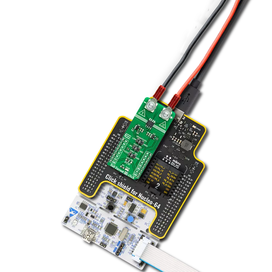
Nucleo 64 with STM32F410RB MCU
Compiler
NECTO Studio
MCU
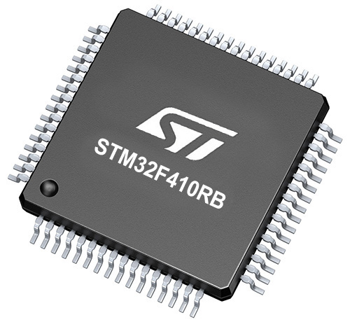
STM32F410RB
Our voltage-to-frequency technology empowers you to seamlessly convert voltage levels into highly accurate frequency signals, setting a new benchmark for signal synthesis and control
A
A
Hardware Overview
How does it work?
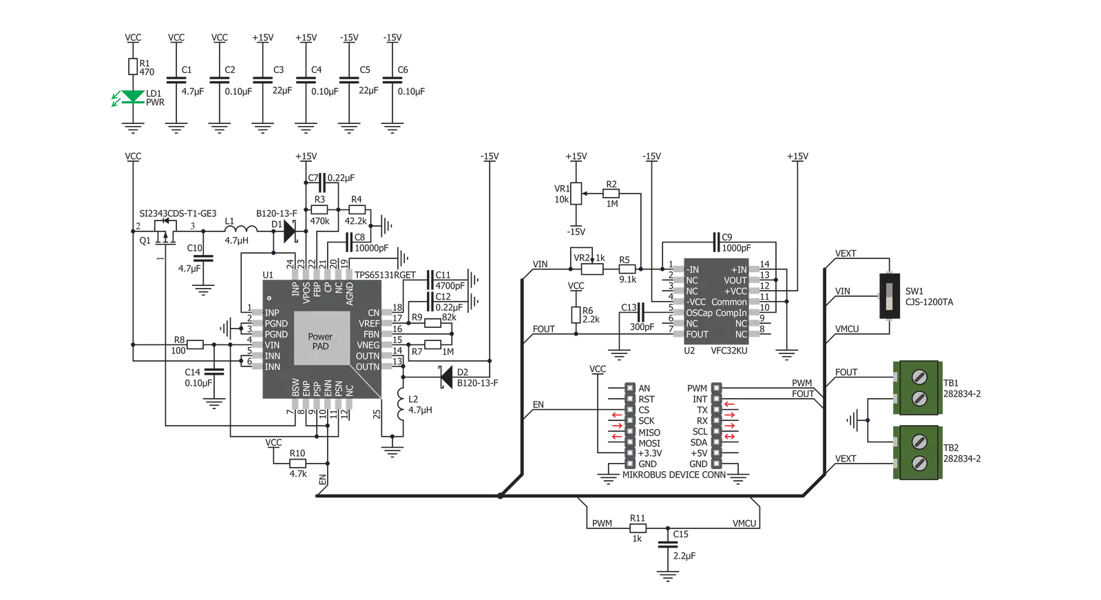
V to Hz 2 Click is based on the VFC32KU, a voltage-to-frequency and frequency-to-voltage converter from Texas Instruments. It accepts voltage at its input and generates a pulse train, with a frequency linearly proportional to the input voltage. The pulse train is routed to a screw terminal labeled as FOUT, as well as the mikroBUS™ INT pin, labeled as FO. The signal can be then further processed by the host MCU. When V to Hz 2 click is operated for the first time, it needs to be calibrated. The click is equipped with two variable resistors for gain and offset fine-tuning. A calibration procedure should be executed before the first use of the Click board™ since even slight variations in the components tolerances could affect the value at the output. It is recommended to correct the offset after longer
time intervals, to compensate for the aging of the passive components on the Click board™. It is done by introducing a known voltage at the input, and adjusting the gain and the offset, until the signal with the expected frequency appears on the output. As already discussed, V to Hz 2 click is equipped with the input voltage terminal (VEXT), which is used to connect the control voltage up to 3.3V. Besides having control voltage input on this terminal, it is possible to select the voltage generated by the MCU as the control voltage input, too. INPUT SEL switch can be set so that the PWM pin from the mikroBUS™ is used as the control voltage input. The PWM signal generated by the MCU is filtered out by the onboard low pass filter so that the control voltage remains constant. The VFC32KU IC requires a dual power supply with
±15V. Therefore, this Click board™ utilizes another IC in order to provide the required voltages. It uses the TPS65131, a positive and negative output DC/DC Converter, from Texas Instruments. This DC/DC converter has already been used in Boost-INV 2 click, so it was tested "on the field" for this purpose. Providing well-stabilized output with the plenty of power headroom, it is a perfect solution for the V to Hz 2 click, also. To enable the conversion circuitry, the EN pin of the TPS65131 boost converter should be pulled to a HIGH logic level. This will activate the boost converter and provide the required power for the VFC32KU IC. This pin is routed to the mikroBUS™ CS pin and it is labeled as EN.

Features overview
Development board
Nucleo-64 with STM32F410RB MCU offers a cost-effective and adaptable platform for developers to explore new ideas and prototype their designs. This board harnesses the versatility of the STM32 microcontroller, enabling users to select the optimal balance of performance and power consumption for their projects. It accommodates the STM32 microcontroller in the LQFP64 package and includes essential components such as a user LED, which doubles as an ARDUINO® signal, alongside user and reset push-buttons, and a 32.768kHz crystal oscillator for precise timing operations. Designed with expansion and flexibility in mind, the Nucleo-64 board features an ARDUINO® Uno V3 expansion connector and ST morpho extension pin
headers, granting complete access to the STM32's I/Os for comprehensive project integration. Power supply options are adaptable, supporting ST-LINK USB VBUS or external power sources, ensuring adaptability in various development environments. The board also has an on-board ST-LINK debugger/programmer with USB re-enumeration capability, simplifying the programming and debugging process. Moreover, the board is designed to simplify advanced development with its external SMPS for efficient Vcore logic supply, support for USB Device full speed or USB SNK/UFP full speed, and built-in cryptographic features, enhancing both the power efficiency and security of projects. Additional connectivity is
provided through dedicated connectors for external SMPS experimentation, a USB connector for the ST-LINK, and a MIPI® debug connector, expanding the possibilities for hardware interfacing and experimentation. Developers will find extensive support through comprehensive free software libraries and examples, courtesy of the STM32Cube MCU Package. This, combined with compatibility with a wide array of Integrated Development Environments (IDEs), including IAR Embedded Workbench®, MDK-ARM, and STM32CubeIDE, ensures a smooth and efficient development experience, allowing users to fully leverage the capabilities of the Nucleo-64 board in their projects.

Microcontroller Overview
MCU Card / MCU
Architecture
ARM Cortex-M4
MCU Memory (KB)
128
Silicon Vendor
STMicroelectronics
Pin count
64
RAM (Bytes)
32768
You complete me!
Accessories
Click Shield for Nucleo-64 comes equipped with two proprietary mikroBUS™ sockets, allowing all the Click board™ devices to be interfaced with the STM32 Nucleo-64 board with no effort. This way, Mikroe allows its users to add any functionality from our ever-growing range of Click boards™, such as WiFi, GSM, GPS, Bluetooth, ZigBee, environmental sensors, LEDs, speech recognition, motor control, movement sensors, and many more. More than 1537 Click boards™, which can be stacked and integrated, are at your disposal. The STM32 Nucleo-64 boards are based on the microcontrollers in 64-pin packages, a 32-bit MCU with an ARM Cortex M4 processor operating at 84MHz, 512Kb Flash, and 96KB SRAM, divided into two regions where the top section represents the ST-Link/V2 debugger and programmer while the bottom section of the board is an actual development board. These boards are controlled and powered conveniently through a USB connection to program and efficiently debug the Nucleo-64 board out of the box, with an additional USB cable connected to the USB mini port on the board. Most of the STM32 microcontroller pins are brought to the IO pins on the left and right edge of the board, which are then connected to two existing mikroBUS™ sockets. This Click Shield also has several switches that perform functions such as selecting the logic levels of analog signals on mikroBUS™ sockets and selecting logic voltage levels of the mikroBUS™ sockets themselves. Besides, the user is offered the possibility of using any Click board™ with the help of existing bidirectional level-shifting voltage translators, regardless of whether the Click board™ operates at a 3.3V or 5V logic voltage level. Once you connect the STM32 Nucleo-64 board with our Click Shield for Nucleo-64, you can access hundreds of Click boards™, working with 3.3V or 5V logic voltage levels.

Used MCU Pins
mikroBUS™ mapper
Take a closer look
Click board™ Schematic
Step by step
Project assembly
Start by selecting your development board and Click board™. Begin with the Nucleo 64 with STM32F410RB MCU as your development board.


Track your results in real time
Application Output
1. Application Output - In Debug mode, the 'Application Output' window enables real-time data monitoring, offering direct insight into execution results. Ensure proper data display by configuring the environment correctly using the provided tutorial.

2. UART Terminal - Use the UART Terminal to monitor data transmission via a USB to UART converter, allowing direct communication between the Click board™ and your development system. Configure the baud rate and other serial settings according to your project's requirements to ensure proper functionality. For step-by-step setup instructions, refer to the provided tutorial.

3. Plot Output - The Plot feature offers a powerful way to visualize real-time sensor data, enabling trend analysis, debugging, and comparison of multiple data points. To set it up correctly, follow the provided tutorial, which includes a step-by-step example of using the Plot feature to display Click board™ readings. To use the Plot feature in your code, use the function: plot(*insert_graph_name*, variable_name);. This is a general format, and it is up to the user to replace 'insert_graph_name' with the actual graph name and 'variable_name' with the parameter to be displayed.

Software Support
Library Description
This library contains API for V To Hz 2 Click driver.
Key functions:
vtohz2_get_freq_out- Function gets the out frequency on mikrobus INT pinvtohz2_enable- Function performs enabling and disabling of the devicevtohz2_pwm_start- This function starts PWM module.
Open Source
Code example
The complete application code and a ready-to-use project are available through the NECTO Studio Package Manager for direct installation in the NECTO Studio. The application code can also be found on the MIKROE GitHub account.
/*!
 * \file
 * \brief VToHz2 Click example
 *
 * # Description
 * This appliaction enables usage of a converter for analog voltage input signal into a pulse wave signal of a certain frequency.
 *
 * The demo application is composed of two sections :
 *
 * ## Application Init
 * Initializes driver and enables the Click board.
 *
 * ## Application Task
 * Sets the output frequency by incrementing the pwm duty cycle from 0 to 100% in an infinite loop.
 * Results are being sent to USB UART terminal.
 *
 * \author MikroE Team
 *
 */
// ------------------------------------------------------------------- INCLUDES

#include "board.h"
#include "log.h"
#include "vtohz2.h"

// ------------------------------------------------------------------ VARIABLES

static vtohz2_t vtohz2;
static log_t logger;

static float duty_cycle = 0.5;

// ------------------------------------------------------ APPLICATION FUNCTIONS

void application_init ( void )
{
    log_cfg_t log_cfg;
    vtohz2_cfg_t cfg;

    /**
     * Logger initialization.
     * Default baud rate: 115200
     * Default log level: LOG_LEVEL_DEBUG
     * @note If USB_UART_RX and USB_UART_TX
     * are defined as HAL_PIN_NC, you will
     * need to define them manually for log to work.
     * See @b LOG_MAP_USB_UART macro definition for detailed explanation.
     */
    LOG_MAP_USB_UART( log_cfg );
    log_init( &logger, &log_cfg );
    log_info( &logger, "---- Application Init ----" );

    //  Click initialization.

    vtohz2_cfg_setup( &cfg );
    VTOHZ2_MAP_MIKROBUS( cfg, MIKROBUS_1 );
    vtohz2_init( &vtohz2, &cfg );

    vtohz2_enable( &vtohz2, VTOHZ2_ENABLE );
    vtohz2_pwm_start( &vtohz2 );
}

void application_task ( void )
{
    for ( duty_cycle = 0; duty_cycle <= 1.0; duty_cycle += 0.01 )
    {
        vtohz2_set_duty_cycle ( &vtohz2, duty_cycle );
        log_printf( &logger," PWM Duty: %.2f%%\r\n", duty_cycle * 100 );
        Delay_ms ( 100 );
    }
    log_printf( &logger, "------------------------------\r\n" );
}

int main ( void )
{
    /* Do not remove this line or clock might not be set correctly. */
    #ifdef PREINIT_SUPPORTED
    preinit();
    #endif

    application_init( );

    for ( ; ; )
    {
        application_task( );
    }

    return 0;
}


// ------------------------------------------------------------------------ END
Additional Support
Resources
Category:Measurements