Navigate current monitoring with confidence using PAC1921 and STM32G474RE
Ultimate solution for accurate and reliable power monitoring

Published Nov 08, 2024
Click board™
PAC1921 Click
Dev. board
Nucleo 64 with STM32G474RE MCU
Compiler
NECTO Studio
MCU
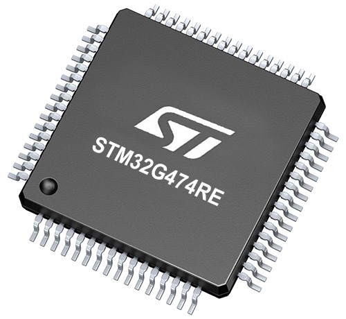
STM32G474RE
Experience a new level of precision with our power monitoring technology, designed for high-side current measurement, ensuring you have the insights you need for critical analysis
A
A
Hardware Overview
How does it work?
PAC1921 Click is based on the PAC1921, a high-side power/current monitor from Microchip. The measurement is done by the SENSE+ and SENSE- pins, which are routed to the onboard terminals used for connecting the load. A shunt resistor of 10mΩ is also soldered between these two pins. The SENSE pins are very sensitive to the voltage and they can detect up to 100mV of across the shunt resistor. The OUT pin of the PAC1921 IC can be used to output an analog voltage, which corresponds to the selected measured electrical property - voltage, current or power. The full scale for the measurement can be set to 1V, 1.5V, 2V and 3V. The OUT pin of the IC is routed to the mikroBUS™ AN pin so that the host MCU can instantly read the measurement information without latency, common for the serial communication. The load should be connected in series with the PAC1921 click so that the positive end of the power supply runs through the PAC1921 click SENSE+ terminal, SENSE- terminal and finally to the positive end of the load. Negative end (GND) of the load is connected to the ground. The voltage drop across the shunt resistor is used to measure the current flow through the load and it should not exceed 6A. When the voltage drop across the shunt resistor and its resistance are known, the current can be easily calculated. The voltage across the connected power supply is measured between the SENSE+ pin and the GND. The maximum voltage level between the SENSE+ and the GND rail should not exceed 32V. During the measurement, these values are stored in the appropriate registers and are used for the power calculation. PAC1921 is able
to integrate the measurements so that the average value can be calculated. The integration can be done in two modes: Free-Run mode and Pin Controlled mode. Pin Controlled integration mode can be engaged by pulling the #READ/INT pin to a HIGH level. This pin is routed to the mikroBUS™ INT pin. The measured type in this mode is limited only to power readings. While the pin is held at a HIGH logic level or before 2048 measuring samples are made, the PAC1921 IC will perform an integration of the measured values. After the integration is over - either after 2048 samples are taken, or after the #READ/INT pin is pulled to a LOW logic level for the minimum update time at any moment, the registers are updated, and the calculated value is sent to the 10bit DAC of the OUT pin. Pulling the #READ/INT pin to a LOW logic level for a minimum update time will put the device into the Read mode, stop the integration process and send the value to the 10bit DAC of the OUT pin. While working in Free-Run integration mode, besides the power measurement, it is possible to measure current and voltage, too. The Free-Run integration time depends on the selected measuring mode, filtering, resolution, and the number of samples, which is selectable to a maximum of 2048 samples. The filtering improves the signal quality but increases the integration time for 50%. Also, when less integration time is required, 11bit ADC conversion should be used instead of the 14bit, at a cost of decreased precision. When power reading mode is selected as the measurement type, both voltage and current registers will be
updated, resulting in longer integration time. While the device stays in the integration mode, the information will be latched on the DAC of the OUT pin after each integration period. When the device enters the Read mode, the integration is interrupted, and the collected data is discarded. The device is able to enter the Read mode by setting the appropriate registers, too. While integrating the measured values, the device will place the selected measured electrical property values into the accumulator registers. At the end of the integration period, this averaged value is sent to the output 10bit DAC of the OUT pin, so that it can be read by the host MCU. It is also available in the registers, in a form of the MSB/LSB and by using conversion formulas from the PAC1921 datasheet, this value can be directly converted to the physical value of the electrical property - ampers [A], volts [V] or watts [W]. All the required setup and config registers are described in the PAC1921 datasheet, in details. This Click board™ library contains functions used to easily set up the device registers and read the measurements for the selected electrical property. The provided demo application can be used as a starting point or a reference for a custom design. PAC1921 click features the onboard SMD jumper, labeled as the PWR SEL, which can be used to set the operating voltage and the logic level for the I2C communication lines so that both 3.3V and 5V capable MCUs can communicate with the device. The communication lines are already equipped with the pull-up resistors so that the device is ready to be used out of the box.

Features overview
Development board
Nucleo-64 with STM32G474R MCU offers a cost-effective and adaptable platform for developers to explore new ideas and prototype their designs. This board harnesses the versatility of the STM32 microcontroller, enabling users to select the optimal balance of performance and power consumption for their projects. It accommodates the STM32 microcontroller in the LQFP64 package and includes essential components such as a user LED, which doubles as an ARDUINO® signal, alongside user and reset push-buttons, and a 32.768kHz crystal oscillator for precise timing operations. Designed with expansion and flexibility in mind, the Nucleo-64 board features an ARDUINO® Uno V3 expansion connector and ST morpho extension pin
headers, granting complete access to the STM32's I/Os for comprehensive project integration. Power supply options are adaptable, supporting ST-LINK USB VBUS or external power sources, ensuring adaptability in various development environments. The board also has an on-board ST-LINK debugger/programmer with USB re-enumeration capability, simplifying the programming and debugging process. Moreover, the board is designed to simplify advanced development with its external SMPS for efficient Vcore logic supply, support for USB Device full speed or USB SNK/UFP full speed, and built-in cryptographic features, enhancing both the power efficiency and security of projects. Additional connectivity is
provided through dedicated connectors for external SMPS experimentation, a USB connector for the ST-LINK, and a MIPI® debug connector, expanding the possibilities for hardware interfacing and experimentation. Developers will find extensive support through comprehensive free software libraries and examples, courtesy of the STM32Cube MCU Package. This, combined with compatibility with a wide array of Integrated Development Environments (IDEs), including IAR Embedded Workbench®, MDK-ARM, and STM32CubeIDE, ensures a smooth and efficient development experience, allowing users to fully leverage the capabilities of the Nucleo-64 board in their projects.

Microcontroller Overview
MCU Card / MCU
Architecture
ARM Cortex-M4
MCU Memory (KB)
512
Silicon Vendor
STMicroelectronics
Pin count
64
RAM (Bytes)
128k
You complete me!
Accessories
Click Shield for Nucleo-64 comes equipped with two proprietary mikroBUS™ sockets, allowing all the Click board™ devices to be interfaced with the STM32 Nucleo-64 board with no effort. This way, Mikroe allows its users to add any functionality from our ever-growing range of Click boards™, such as WiFi, GSM, GPS, Bluetooth, ZigBee, environmental sensors, LEDs, speech recognition, motor control, movement sensors, and many more. More than 1537 Click boards™, which can be stacked and integrated, are at your disposal. The STM32 Nucleo-64 boards are based on the microcontrollers in 64-pin packages, a 32-bit MCU with an ARM Cortex M4 processor operating at 84MHz, 512Kb Flash, and 96KB SRAM, divided into two regions where the top section represents the ST-Link/V2 debugger and programmer while the bottom section of the board is an actual development board. These boards are controlled and powered conveniently through a USB connection to program and efficiently debug the Nucleo-64 board out of the box, with an additional USB cable connected to the USB mini port on the board. Most of the STM32 microcontroller pins are brought to the IO pins on the left and right edge of the board, which are then connected to two existing mikroBUS™ sockets. This Click Shield also has several switches that perform functions such as selecting the logic levels of analog signals on mikroBUS™ sockets and selecting logic voltage levels of the mikroBUS™ sockets themselves. Besides, the user is offered the possibility of using any Click board™ with the help of existing bidirectional level-shifting voltage translators, regardless of whether the Click board™ operates at a 3.3V or 5V logic voltage level. Once you connect the STM32 Nucleo-64 board with our Click Shield for Nucleo-64, you can access hundreds of Click boards™, working with 3.3V or 5V logic voltage levels.

Used MCU Pins
mikroBUS™ mapper
Take a closer look
Click board™ Schematic

Step by step
Project assembly
Start by selecting your development board and Click board™. Begin with the Nucleo 64 with STM32G474RE MCU as your development board.


Track your results in real time
Application Output
1. Application Output - In Debug mode, the 'Application Output' window enables real-time data monitoring, offering direct insight into execution results. Ensure proper data display by configuring the environment correctly using the provided tutorial.

2. UART Terminal - Use the UART Terminal to monitor data transmission via a USB to UART converter, allowing direct communication between the Click board™ and your development system. Configure the baud rate and other serial settings according to your project's requirements to ensure proper functionality. For step-by-step setup instructions, refer to the provided tutorial.

3. Plot Output - The Plot feature offers a powerful way to visualize real-time sensor data, enabling trend analysis, debugging, and comparison of multiple data points. To set it up correctly, follow the provided tutorial, which includes a step-by-step example of using the Plot feature to display Click board™ readings. To use the Plot feature in your code, use the function: plot(*insert_graph_name*, variable_name);. This is a general format, and it is up to the user to replace 'insert_graph_name' with the actual graph name and 'variable_name' with the parameter to be displayed.

Software Support
Library Description
This library contains API for PAC1921 Click driver.
Key functions:
pac1921_write_to_reg- This function writes data to the specified register address/es and saves the state of the register/s so it doesn't write the same value/s twicepac1921_get_measured_data- This function gathers voltage/power data from the PAC1921 chip and, depending on the measurement mode, converts those raw values into a more suitable formpac1921_set_int_pin- This function sets the digital output on the interrupt pin.
Open Source
Code example
The complete application code and a ready-to-use project are available through the NECTO Studio Package Manager for direct installation in the NECTO Studio. The application code can also be found on the MIKROE GitHub account.
/*!
 * \file
 * \brief PAC1921 Click example
 *
 * # Description
 * This example showcases how to measure voltage, current or power (load) data using the
 * PAC1921 chip. Required modules are first initialized and after used to read and
 * display the measured data.
 *
 * The demo application is composed of two sections :
 *
 * ## Application Init
 * This function initializes and configures the logger and Click modules. Default settings
 * are written to three control/configuration registers in the default_cfg(...) function.
 *
 * ## Application Task
 * This function reads and displays voltage, current or power data from the chip, depending
 * on the specified measurement mode and sample count. It does so every half a second.
 *
 * \author MikroE Team
 *
 */
// ------------------------------------------------------------------- INCLUDES

#include "board.h"
#include "log.h"
#include "pac1921.h"

// ------------------------------------------------------------------ VARIABLES

static pac1921_t pac1921;
static log_t logger;

// ------------------------------------------------------ APPLICATION FUNCTIONS

void application_init ( )
{
    log_cfg_t log_cfg;
    pac1921_cfg_t cfg;

    /**
     * Logger initialization.
     * Default baud rate: 115200
     * Default log level: LOG_LEVEL_DEBUG
     * @note If USB_UART_RX and USB_UART_TX
     * are defined as HAL_PIN_NC, you will
     * need to define them manually for log to work.
     * See @b LOG_MAP_USB_UART macro definition for detailed explanation.
     */
    LOG_MAP_USB_UART( log_cfg );
    log_init( &logger, &log_cfg );
    log_info( &logger, "---- Application Init ----" );

    //  Click initialization.

    pac1921_cfg_setup( &cfg );
    PAC1921_MAP_MIKROBUS( cfg, MIKROBUS_1 );
    pac1921_init( &pac1921, &cfg );
    Delay_ms ( 100 );
    pac1921_default_cfg( &pac1921 );
    Delay_ms ( 100 );
}

void application_task ( )
{
    float read_data;

    read_data = pac1921_get_measured_data( &pac1921, PAC1921_MEASUREMENT_MODE_V_BUS_FREE_RUN,
                                                     PAC1921_SAMPLE_RATE_512 );

    if ( pac1921.aux.measurement_mode_old == PAC1921_MEASUREMENT_MODE_V_POWER_FREE_RUN )
    {
        log_printf( &logger, " * Power: %.2f W * \r\n", read_data );
    }
    else
    {
        log_printf( &logger, " * Voltage: %.2f mV * \r\n", read_data );
    }

    Delay_ms ( 500 );
}

int main ( void )
{
    /* Do not remove this line or clock might not be set correctly. */
    #ifdef PREINIT_SUPPORTED
    preinit();
    #endif

    application_init( );

    for ( ; ; )
    {
        application_task( );
    }

    return 0;
}

// ------------------------------------------------------------------------ END


