Convert analog signals into precise digital values with ADS1015L and PIC18F57Q43
Delta-sigma (ΔΣ) 12-bit analog-to-digital converter with an I2C-compatible interface

Published Dec 18, 2024
Click board™
ADC 26 Click
Dev. board
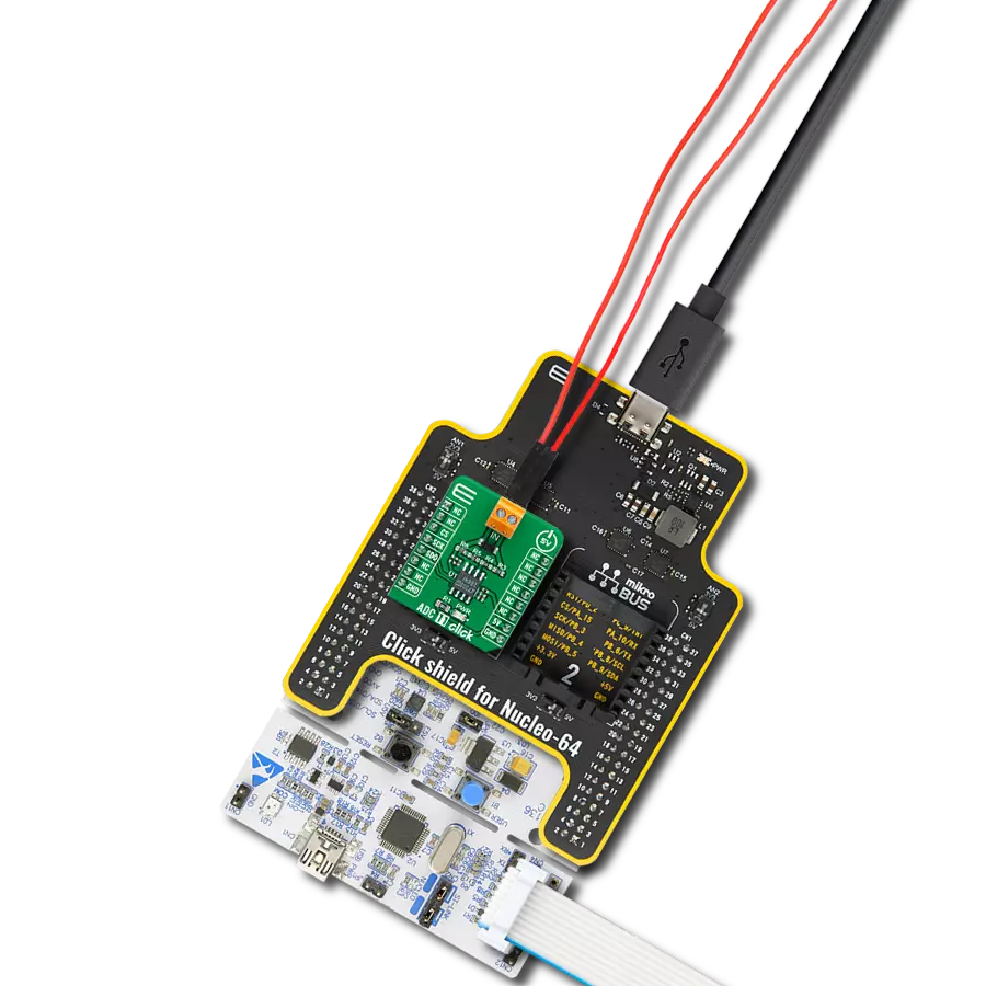
Curiosity Nano with PIC18F57Q43
Compiler
NECTO Studio
MCU
PIC18F57Q43
Low-power 12-bit analog-to-digital conversion for real-time performance in system monitoring and current sensing
A
A
Hardware Overview
How does it work?
ADC 26 Click is based on the ADS1015L, a low-power 12-bit analog-to-digital converter (ADC) with an I2C-compatible interface from Texas Instruments. It integrates several key components: a ΔΣ ADC core, an internal voltage reference, a clock oscillator, a programmable gain amplifier (PGA), and a programmable digital comparator. This combination enables the ADC to deliver conversions at data rates of up to 3300 samples per second (SPS), making it suitable for applications requiring both high speed and low noise. The ADC core of the ADS1015L measures differential signals brought to its analog input channels (IN0-IN3), offering a flexible full-scale input voltage range from ±0.256V to ±6.144V. This broad range enables the ADS1015L to handle both large and small signals with high precision, making it ideal for general system monitoring tasks such as supply voltage tracking, current sensing, and temperature measurements. These features also cater to applications in wearables and personal electronics. The IC's architecture comprises a differential switched-capacitor ΔΣ modulator followed by a digital filter, ensuring excellent attenuation of common-mode signals and high immunity to noise. The input signal is compared
against the internal voltage reference, while the modulator generates a high-speed bitstream. This stream is processed by the digital filter, which produces a digital output code proportional to the measured voltage. The ADS1015L supports two operational modes designed to optimize power consumption and performance based on application requirements. In single-shot mode, the ADC executes a single measurement upon request, stores the result in an internal register, and then enters a power-down state, making it particularly effective for systems that require periodic measurements or experience extended idle periods between conversions. In continuous-conversion mode, the ADC seamlessly initiates a new measurement as soon as the previous one is completed, maintaining a conversion rate consistent with the configured data rate. This mode is well-suited for real-time monitoring applications, as the data register consistently contains the most recent measurement. This Click board™ is designed in a unique format supporting the newly introduced MIKROE feature called "Click Snap." Unlike the standardized version of Click boards, this feature allows the main IC area to become movable by breaking the PCB, opening up many
new possibilities for implementation. Thanks to the Snap feature, the ADS1015l can operate autonomously by accessing its signals directly on the pins marked 1-8. Additionally, the Snap part includes a specified and fixed screw hole position, enabling users to secure the Snap board in their desired location. ADC 26 Click uses an I2C interface with clock speeds of up to 400kHz, ensuring fast and efficient communication with the host MCU. The I2C address can be easily configured via onboard ADDR SEL jumpers positioned in the Snap part of the board, allowing multiple devices to coexist on the same bus. Additionally, the board features an alert interrupt (AR) pin triggered whenever conversion data exceeds the limit set in the appropriate upper/lower threshold register, or it can be used as a conversion-ready pin. This Click board™ can be operated only with a 3.3V logic voltage level. The board must perform appropriate logic voltage level conversion before using MCUs with different logic levels. It also comes equipped with a library containing functions and example code that can be used as a reference for further development.

Features overview
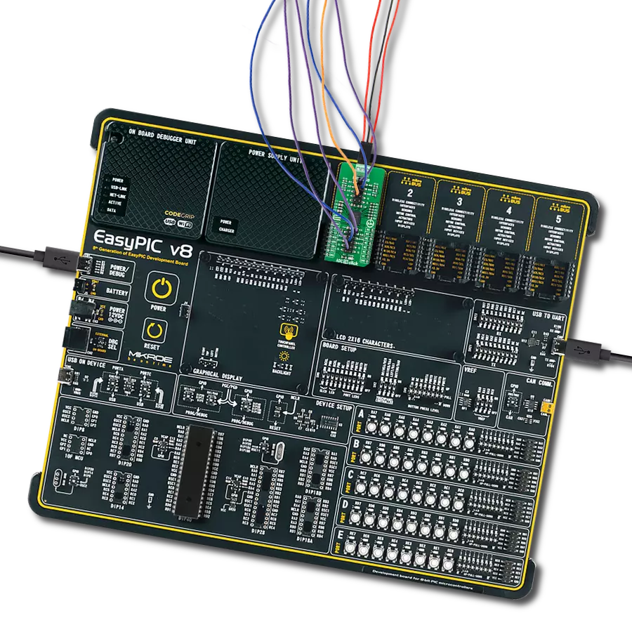
Development board
PIC18F57Q43 Curiosity Nano evaluation kit is a cutting-edge hardware platform designed to evaluate microcontrollers within the PIC18-Q43 family. Central to its design is the inclusion of the powerful PIC18F57Q43 microcontroller (MCU), offering advanced functionalities and robust performance. Key features of this evaluation kit include a yellow user LED and a responsive
mechanical user switch, providing seamless interaction and testing. The provision for a 32.768kHz crystal footprint ensures precision timing capabilities. With an onboard debugger boasting a green power and status LED, programming and debugging become intuitive and efficient. Further enhancing its utility is the Virtual serial port (CDC) and a debug GPIO channel (DGI
GPIO), offering extensive connectivity options. Powered via USB, this kit boasts an adjustable target voltage feature facilitated by the MIC5353 LDO regulator, ensuring stable operation with an output voltage ranging from 1.8V to 5.1V, with a maximum output current of 500mA, subject to ambient temperature and voltage constraints.

Microcontroller Overview
MCU Card / MCU

Architecture
PIC
MCU Memory (KB)
128
Silicon Vendor
Microchip
Pin count
48
RAM (Bytes)
8196
You complete me!
Accessories
Curiosity Nano Base for Click boards is a versatile hardware extension platform created to streamline the integration between Curiosity Nano kits and extension boards, tailored explicitly for the mikroBUS™-standardized Click boards and Xplained Pro extension boards. This innovative base board (shield) offers seamless connectivity and expansion possibilities, simplifying experimentation and development. Key features include USB power compatibility from the Curiosity Nano kit, alongside an alternative external power input option for enhanced flexibility. The onboard Li-Ion/LiPo charger and management circuit ensure smooth operation for battery-powered applications, simplifying usage and management. Moreover, the base incorporates a fixed 3.3V PSU dedicated to target and mikroBUS™ power rails, alongside a fixed 5.0V boost converter catering to 5V power rails of mikroBUS™ sockets, providing stable power delivery for various connected devices.

Used MCU Pins
mikroBUS™ mapper
Take a closer look
Click board™ Schematic

Step by step
Project assembly

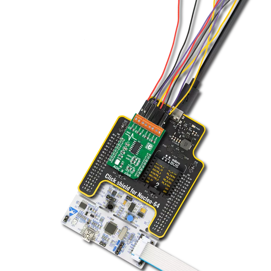
Start by selecting your development board and Click board™. Begin with the Curiosity Nano with PIC18F57Q43 as your development board.


Track your results in real time
Application Output
1. Application Output - In Debug mode, the 'Application Output' window enables real-time data monitoring, offering direct insight into execution results. Ensure proper data display by configuring the environment correctly using the provided tutorial.

2. UART Terminal - Use the UART Terminal to monitor data transmission via a USB to UART converter, allowing direct communication between the Click board™ and your development system. Configure the baud rate and other serial settings according to your project's requirements to ensure proper functionality. For step-by-step setup instructions, refer to the provided tutorial.

3. Plot Output - The Plot feature offers a powerful way to visualize real-time sensor data, enabling trend analysis, debugging, and comparison of multiple data points. To set it up correctly, follow the provided tutorial, which includes a step-by-step example of using the Plot feature to display Click board™ readings. To use the Plot feature in your code, use the function: plot(*insert_graph_name*, variable_name);. This is a general format, and it is up to the user to replace 'insert_graph_name' with the actual graph name and 'variable_name' with the parameter to be displayed.

Software Support
Library Description
This library contains API for ADC 26 Click driver.
Key functions:
adc26_start_conversion- This function starts a single-shot conversion for the selected MUX channel and gain level (full-scale range).adc26_get_alert_pin- This function returns the ALERT (data ready) pin logic state.adc26_read_voltage- This function reads the RAW ADC measurement and converts it to a voltage level.
Open Source
Code example
The complete application code and a ready-to-use project are available through the NECTO Studio Package Manager for direct installation in the NECTO Studio. The application code can also be found on the MIKROE GitHub account.
/*!
 * @file main.c
 * @brief ADC 26 Click example
 *
 * # Description
 * This example demonstrates the use of ADC 26 Click board by reading and
 * displaying the voltage levels from IN0-IN1 differential and IN2-IN3
 * single-ended analog input channels.
 *
 * The demo application is composed of two sections :
 *
 * ## Application Init
 * Initializes the driver and performs the Click default configuration.
 *
 * ## Application Task
 * Reads the voltage levels from IN0-IN1 differential (+/- 2.048V) and
 * IN2-IN3 single-ended (+/- 4.096V) analog input channels and displays
 * the results on the USB UART once per second approximately.
 *
 * @note
 * Do not apply more than VCC + 0.3 V to the analog inputs of the device.
 *
 * @author Stefan Filipovic
 *
 */

#include "board.h"
#include "log.h"
#include "adc26.h"

static adc26_t adc26;
static log_t logger;

void application_init ( void )
{
    log_cfg_t log_cfg;  /**< Logger config object. */
    adc26_cfg_t adc26_cfg;  /**< Click config object. */

    /**
     * Logger initialization.
     * Default baud rate: 115200
     * Default log level: LOG_LEVEL_DEBUG
     * @note If USB_UART_RX and USB_UART_TX
     * are defined as HAL_PIN_NC, you will
     * need to define them manually for log to work.
     * See @b LOG_MAP_USB_UART macro definition for detailed explanation.
     */
    LOG_MAP_USB_UART( log_cfg );
    log_init( &logger, &log_cfg );
    log_info( &logger, " Application Init " );

    // Click initialization.
    adc26_cfg_setup( &adc26_cfg );
    ADC26_MAP_MIKROBUS( adc26_cfg, MIKROBUS_1 );
    if ( I2C_MASTER_ERROR == adc26_init( &adc26, &adc26_cfg ) )
    {
        log_error( &logger, " Communication init." );
        for ( ; ; );
    }

    if ( ADC26_ERROR == adc26_default_cfg ( &adc26 ) )
    {
        log_error( &logger, " Default configuration." );
        for ( ; ; );
    }

    log_info( &logger, " Application Task " );
}

void application_task ( void )
{
    float voltage = 0;
    if ( ADC26_OK == adc26_start_conversion ( &adc26, ADC26_MUX_P_AIN0_N_AIN1, ADC26_PGA_2_048V ) )
    {
        while ( adc26_get_alert_pin ( &adc26 ) ); // Waits for a data ready indication

        if ( ADC26_OK == adc26_read_voltage ( &adc26, &voltage ) )
        {
            log_printf ( &logger, " Voltage between IN0[P] and IN1[N]: %.3f V\r\n", voltage );
        }
    }
    if ( ADC26_OK == adc26_start_conversion ( &adc26, ADC26_MUX_P_AIN2_N_GND, ADC26_PGA_4_096V ) )
    {
        while ( adc26_get_alert_pin ( &adc26 ) ); // Waits for a data ready indication

        if ( ADC26_OK == adc26_read_voltage ( &adc26, &voltage ) )
        {
            log_printf ( &logger, " Voltage between IN2 and GND: %.3f V\r\n", voltage );
        }
    }
    if ( ADC26_OK == adc26_start_conversion ( &adc26, ADC26_MUX_P_AIN3_N_GND, ADC26_PGA_4_096V ) )
    {
        while ( adc26_get_alert_pin ( &adc26 ) ); // Waits for a data ready indication

        if ( ADC26_OK == adc26_read_voltage ( &adc26, &voltage ) )
        {
            log_printf ( &logger, " Voltage between IN3 and GND: %.3f V\r\n\n", voltage );
        }
    }
    Delay_ms ( 1000 );
}

int main ( void )
{
    /* Do not remove this line or clock might not be set correctly. */
    #ifdef PREINIT_SUPPORTED
    preinit();
    #endif

    application_init( );

    for ( ; ; )
    {
        application_task( );
    }

    return 0;
}

// ------------------------------------------------------------------------ END
Additional Support
Resources
Category:ADC