Shape your signals with AD9834 and MK51DN512CLQ10
Frequency stimulus/waveform generation

Published May 27, 2023
Click board™
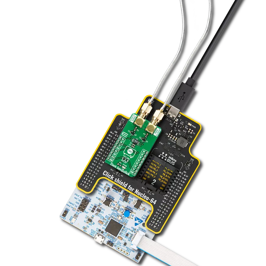
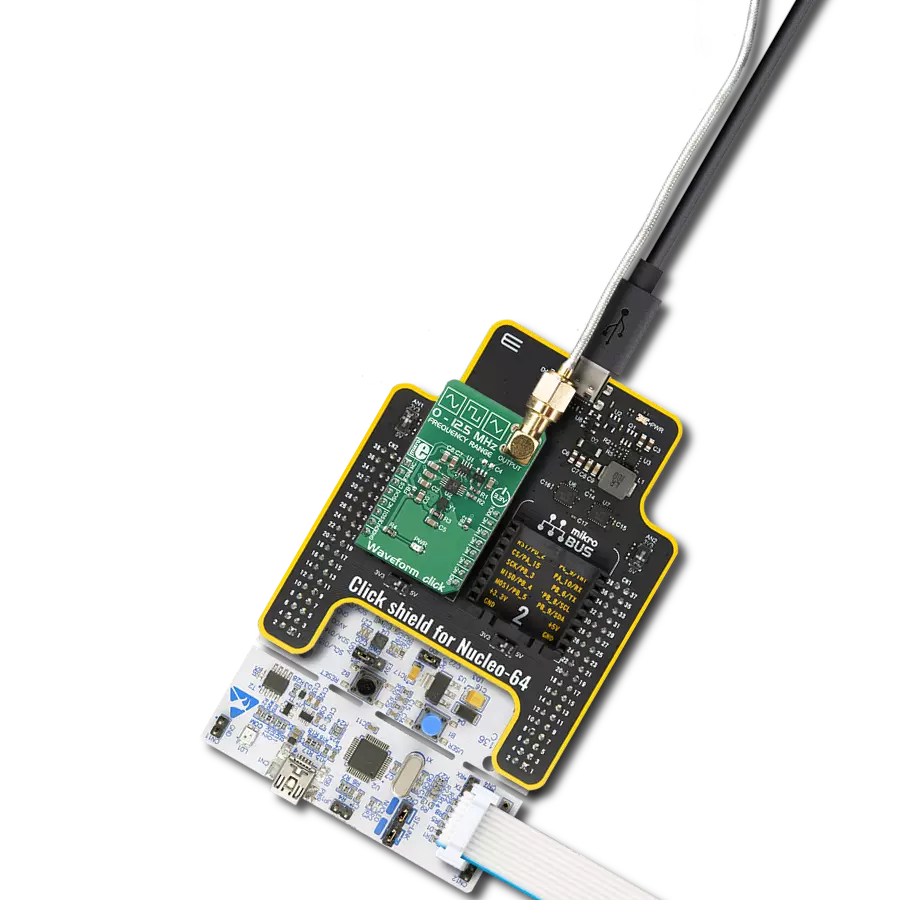
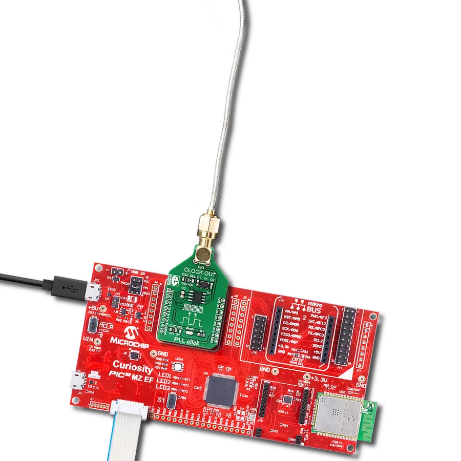
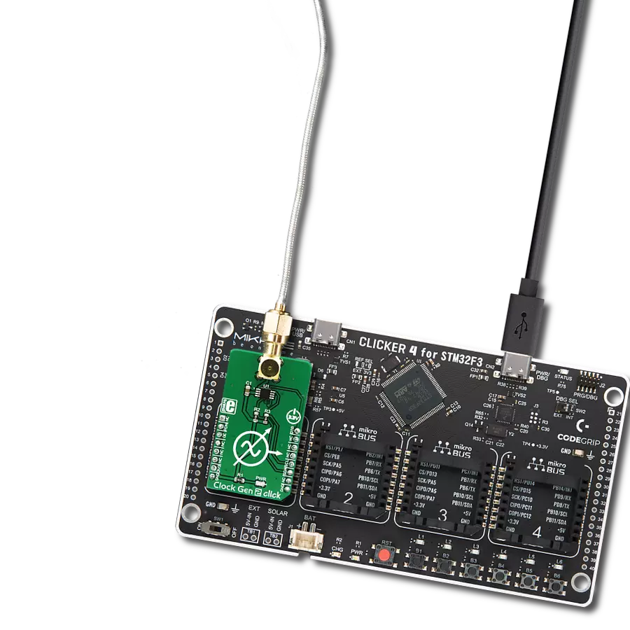
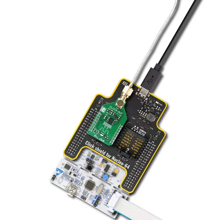
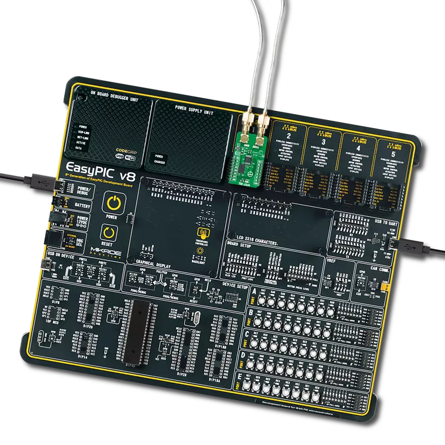
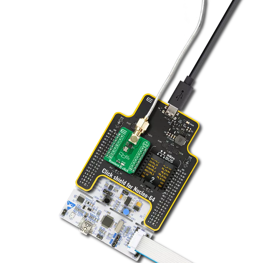
Waveform 2 Click
Dev. board
UNI-DS v8
Compiler
NECTO Studio
MCU
MK51DN512CLQ10
Achieve sine and triangular outputs alongside frequency phase tuning and modulation with an advanced waveform generator
A
A
Hardware Overview
How does it work?
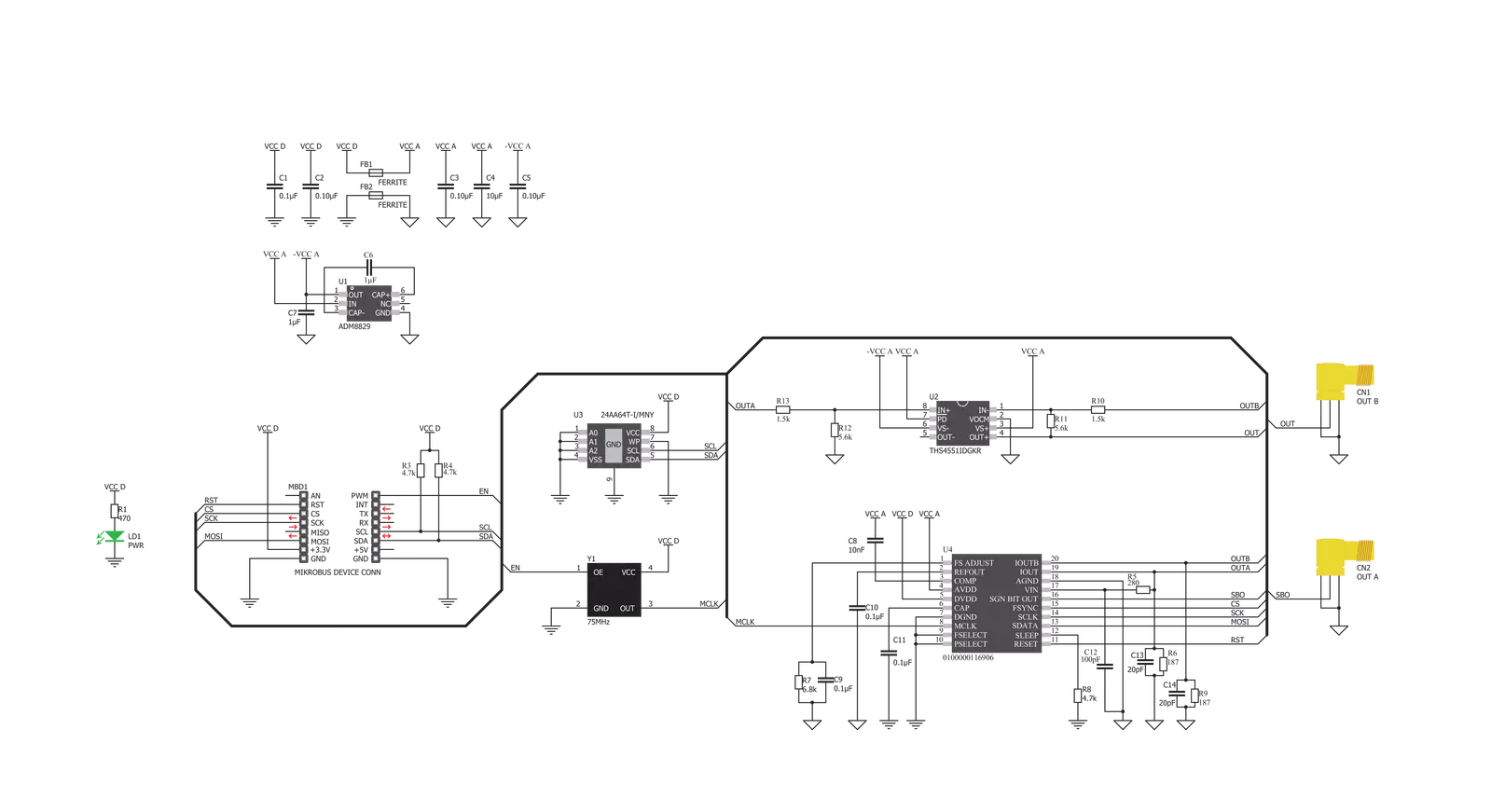
Waveform 2 Click is based on the AD9834, a 75 MHz low-power DDS device capable of producing high-performance sine/triangle/square outputs from Analog Devices. The AD9834 can have a broad range of simple and complex modulation schemes. These modulation schemes are fully implemented in the digital domain, allowing the accurate realization of complex modulation algorithms using DSP techniques. It contains a 16-bit control register accessible through the SPI serial interface that sets up the AD9834 as the user wants to operate it. The internal circuitry of the AD9834 consists of a numerically controlled oscillator (NCO), frequency and phase modulators, SIN ROM, a DAC, a comparator, and a regulator. The outputs of the AD9834 are filtered by an RC network and then amplified via THS4551, a differential amplifier that offers an easy interface from single-ended sources to the differential output required by high-precision
analog-to-digital converters from Texas Instruments.The output signal from the AD9834 follows two paths. One path is routed to an output connector labeled as Signal Out when the output waveform of the generator is sinusoidal or triangular, while the other path, routed to an output connector labeled as Square Out, is used when the output waveform of the generator is square. In addition to the positive supply voltage requirement, the THS4551 amplifier also has a negative supply voltage, achieved by the ADM8829, a charge-pump voltage inverter used to generate a negative supply from a positive input from Analog Devices. This Click board™ also has an external oscillator of 75MHz, enabled by the EN pin of the mikroBUS™ socket, and represents the maximum frequency that the AD9834 can accept. The 75MHz clock produces the cleanest possible Sine waveform at high frequencies, while the low frequencies create
errors. In addition to these features, the Waveform 2 Click also has an EEPROM memory IC the 24AA64, an i2C configurable 64K serial EEPROM from Microchip that can be used for various storage applications. The Waveform 2 Click communicates with MCU using the 3-Wire SPI serial interface compatible with standard SPI, QSPI™, and MICROWIRE™ and operates at clock rates up to 40 MHz. Besides, it possesses additional functionality such as reset function, necessary during AD9834 initialization, implemented and routed at the RST pin of the mikroBUS™ socket. This Click board™ can only be operated with a 3.3V logic voltage level. The board must perform appropriate logic voltage level conversion before using MCUs with different logic levels. However, the Click board™ comes equipped with a library containing functions and an example code that can be used as a reference for further development.


Features overview
Development board
UNI-DS v8 is a development board specially designed for the needs of rapid development of embedded applications. It supports a wide range of microcontrollers, such as different STM32, Kinetis, TIVA, CEC, MSP, PIC, dsPIC, PIC32, and AVR MCUs regardless of their number of pins, and a broad set of unique functions, such as the first-ever embedded debugger/programmer over WiFi. The development board is well organized and designed so that the end-user has all the necessary elements, such as switches, buttons, indicators, connectors, and others, in one place. Thanks to innovative manufacturing technology, UNI-DS v8 provides a fluid and immersive working experience, allowing access anywhere and under any
circumstances at any time. Each part of the UNI-DS v8 development board contains the components necessary for the most efficient operation of the same board. An advanced integrated CODEGRIP programmer/debugger module offers many valuable programming/debugging options, including support for JTAG, SWD, and SWO Trace (Single Wire Output)), and seamless integration with the Mikroe software environment. Besides, it also includes a clean and regulated power supply module for the development board. It can use a wide range of external power sources, including a battery, an external 12V power supply, and a power source via the USB Type-C (USB-C) connector. Communication options such as USB-UART, USB
HOST/DEVICE, CAN (on the MCU card, if supported), and Ethernet is also included. In addition, it also has the well-established mikroBUS™ standard, a standardized socket for the MCU card (SiBRAIN standard), and two display options for the TFT board line of products and character-based LCD. UNI-DS v8 is an integral part of the Mikroe ecosystem for rapid development. Natively supported by Mikroe software tools, it covers many aspects of prototyping and development thanks to a considerable number of different Click boards™ (over a thousand boards), the number of which is growing every day.

Microcontroller Overview
MCU Card / MCU
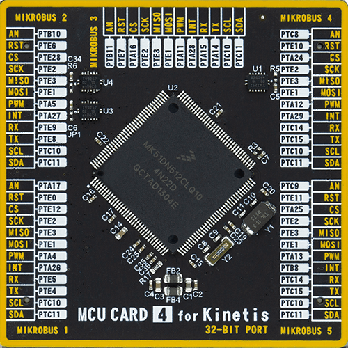
Type
8th Generation
Architecture
ARM Cortex-M4
MCU Memory (KB)
512
Silicon Vendor
NXP
Pin count
144
RAM (Bytes)
131072
Used MCU Pins
mikroBUS™ mapper
Take a closer look
Click board™ Schematic
Step by step
Project assembly

Start by selecting your development board and Click board™. Begin with the UNI-DS v8 as your development board.


Software Support
Library Description
This library contains API for Waveform 2 Click driver.
Key functions:
void waveform2_set_freq ( uint32_t freq )- Function for setting the output frequency.void waveform2_sine_output ( void )- Function for setting the sine output.void waveform2_triangle_output ( void )- Function for setting the triangle output.
Open Source
Code example
The complete application code and a ready-to-use project are available through the NECTO Studio Package Manager for direct installation in the NECTO Studio. The application code can also be found on the MIKROE GitHub account.
/*!
 * @file main.c
 * @brief Waveform2 Click example
 *
 * # Description
 * This is an example that demonstrates the use of the Waveform 2 Click board.
 *
 * The demo application is composed of two sections :
 *
 * ## Application Init
 * Initialize the communication interface, preforming hardware reset, and configure the Click board.
 *
 * ## Application Task
 * Predefined characters are inputed from the serial port.
 * Depending on the character sent the signal frequency, waveform or amplitude
 * will be changed.
 *
 * - Command:
 * [ + ] - Increase frequency
 * [ - ] - Decrease frequency
 * [ t ] - Triangle-shaped signal
 * [ s ] - The signal in the form of a sinusoid
 *
 * - Additional Functions :
 * aprox_freq_calculation( float freqency ) - This function is used to calculate the aproximate
 * value that will be written to the frequency set register.
 *
 * @author Stefan Ilic
 *
 */

#include "board.h"
#include "log.h"
#include "waveform2.h"

static waveform2_t waveform2;
static log_t logger;

float value = 100000;
char demo_rx_buf[ 10 ];
char demo_tx_buf[ 10 ] = "MikroE";

/**
 * @brief Aproximate frequency calculation function.
 * @details This function is used to calculate the aproximate value that will be
 * written to the frequency set register..
 */
uint32_t aprox_freq_calculation ( float freqency );

void application_init ( void ) {
    log_cfg_t log_cfg;  /**< Logger config object. */
    waveform2_cfg_t waveform2_cfg;  /**< Click config object. */

    /**
     * Logger initialization.
     * Default baud rate: 115200
     * Default log level: LOG_LEVEL_DEBUG
     * @note If USB_UART_RX and USB_UART_TX
     * are defined as HAL_PIN_NC, you will
     * need to define them manually for log to work.
     * See @b LOG_MAP_USB_UART macro definition for detailed explanation.
     */
    LOG_MAP_USB_UART( log_cfg );
    log_init( &logger, &log_cfg );
    log_info( &logger, " Application Init " );

    // Click initialization.
    waveform2_cfg_setup( &waveform2_cfg );
    WAVEFORM2_MAP_MIKROBUS( waveform2_cfg, MIKROBUS_1 );
    err_t init_flag  = waveform2_init( &waveform2, &waveform2_cfg );
    if ( ( I2C_MASTER_ERROR == init_flag ) || ( SPI_MASTER_ERROR == init_flag ) ) {
        log_error( &logger, " Application Init Error. " );
        log_info( &logger, " Please, run program again... " );

        for ( ; ; );
    }
    waveform2_default_cfg ( &waveform2 );

    log_printf( &logger, "---- EEPROM test ----\r\n " );
    log_printf( &logger, ">> Write [MikroE] to address 0x0123\r\n " );
    waveform2_eeprom_write_string( &waveform2, 0x0123, demo_tx_buf, 6 );
    waveform2_eeprom_read_string ( &waveform2, 0x0123, demo_rx_buf, 6 );
    log_printf( &logger, ">> Read data: %s  from address 0x0123.... \r\n ", demo_rx_buf );
    Delay_ms ( 1000 );
    waveform2_hw_reset( &waveform2 );
    Delay_ms ( 1000 );

    log_printf( &logger, "---- Waveform set freqency ----\r\n" );
    int32_t freqency;
    freqency = aprox_freq_calculation( value );
    waveform2_set_freq( &waveform2, freqency );
    waveform2_triangle_output( &waveform2 );
    Delay_ms ( 1000 );
    log_info( &logger, " Application Task " );
}

void application_task ( void ) {
    char rx_data;
    uint32_t freq_data;

    if ( log_read( &logger, &rx_data, 1 ) ) {
        switch ( rx_data ) {
            case '+': {
                if ( value > 200000 ) {
                    value = 0;
                }
                value += 100000;
                freq_data = aprox_freq_calculation( value );
                waveform2_set_freq( &waveform2, freq_data );
                log_printf( &logger, ">> Increasing the frequency \r\n " );
                break;
            }

            case '-': {
                if ( value < 200000 ) {
                    value = 400000;
                }
                value -= 100000;
                freq_data = aprox_freq_calculation( value );
                waveform2_set_freq( &waveform2, freq_data );
                log_printf( &logger, ">> Decreasing the frequency \r\n " );
                break;
            }

            case 't': {
                waveform2_triangle_output( &waveform2 );
                log_printf( &logger, ">> Triangle output \r\n " );
                break;
            }

            case 's': {
                waveform2_sine_output( &waveform2 );
                log_printf( &logger,  ">> Sinusoid output \r\n " );
                break;
            }
        }
    }
}

int main ( void )
{
    /* Do not remove this line or clock might not be set correctly. */
    #ifdef PREINIT_SUPPORTED
    preinit();
    #endif

    application_init( );

    for ( ; ; )
    {
        application_task( );
    }

    return 0;
}

uint32_t aprox_freq_calculation ( float freqency ) {
    uint32_t calculation;
    float WAVEFORM_OSC_FREQ = 50000000.0;
    float WAVEFORM_CONSTANT = 268435456.0;

    calculation = freqency * ( WAVEFORM_CONSTANT / WAVEFORM_OSC_FREQ );

    return calculation;
}

// ------------------------------------------------------------------------ END