Create a highly compact, high-performance DAQ solution with ADAQ7768-1 and STM32L073RZ
Streamline data collection - save time and effort
Published Jun 01, 2023
Click board™
DAQ Click
Dev. board
Fusion for STM32 v8
Compiler
NECTO Studio
MCU
STM32L073RZ
Simplify complex data acquisition challenges with our user-friendly solution
A
A
Hardware Overview
How does it work?
DAQ Click is based on the ADAQ7768-1, a 24-bit precision data acquisition μModule system that encapsulates signal conditioning, conversion, and processing blocks into one SiP from Analog Devices, enabling rapid development of highly compact, high-performance precision DAQ systems. The ADAQ7768-1 consists of low noise, high bandwidth programmable gain instrumentation amplifier (PGIA) capable of amplifying and attenuating while maintaining high input impedance. Also, it has a linear phase anti-aliasing filter, a high-performance 24-bit sigma-delta ADC with a programmable digital filter, a low dropout linear regulator, reference buffers, and critical passive components required for the signal chain. The wide common-mode input range of the ADAQ7768-1 allows it to accept a wide variety of signal swings. It supports a fully differential input signal connection with a maximum voltage range of ±12V with an excellent common-mode rejection ratio. The input signal is fully buffered with a low input bias current, enabling the ADAQ7768-1 to directly interface to sensors with high output impedance. The ADAQ7768-1‘s PGA requires a voltage of ±15V to supply the frontend amplifiers. Therefore, a dual-channel low-noise bias generator, the LT3095 from Analog Devices, provides a +15V out of 3V3 mikroBUS™ rail.
A -15V supply is obtained by combining a step-down regulator ADP2300 and a small low-noise LDO ADP7182, both from Analog Devices, also out of 3V3 mikroBUS™ rail. The PGIA has six gain settings capable of varying input ranges from ±0.197V to ±12.603V fully differential input signal, which can be configured with GAIN pins controlled by three multifunction GPIO pins of the ADAQ7768-1 (MODE1-3). An integrated 4th-order low-pass analog filter combined with the user-programmable digital filter ensures the signal chain is fully protected against the high-frequency noise and out-of-band tones presented at the input node. This filter is designed to achieve high phase linearity and maximum in-band magnitude response flatness. Inside the ADAQ7768-1 is a high-performance, 24-bit precision, single-channel Sigma-Delta converter with excellent AC performance and DC precision and throughput rate of 256kSPS from a 16.384MHz onboard crystal (clock source). In addition to the internal clock source, the user can use an external clock brought to the connector labeled as EXT CLK. The clock source is selected by positioning a jumper marked as INT/EXT. Since the LT3095 generates two independent supplies, in addition to -15V, this regulator also provides the 5.3V voltage required to power the internal LDO of the ADAQ7768-1, whose output
supplies an onboard voltage reference - the ADR4540. This Click board™ also allows the user to filter the reference voltage itself, with the optional use of a reference buffer implemented using OpAmp, ADA4807-1, which provides high-speed performance with DC precision, low noise distortion, and power to maintain the accuracy of the reference. This Click board™ communicates with MCU through a standard SPI interface to program the internal registers for complete control of the ADAQ7768-1. In addition, it uses several GPIO pins, such as the reset pin routed to the RST pin on the mikroBUS™ socket, which with a low logic level puts the module into a Reset state, an additional data-ready signal, routed on the INT pin of the mikroBUS™ socket labeled as RDY, indicating that new data is ready for the host, and one extra user-configurable general-purpose I/O pin labeled as IO3 routed to the PWM pin on the mikroBUS™ socket. This Click board™ can only be operated with a 3.3V logic voltage level. The board must perform appropriate logic voltage level conversion before using MCUs with different logic levels. However, the Click board™ comes equipped with a library containing functions and an example code that can be used as a reference for further development.

Features overview
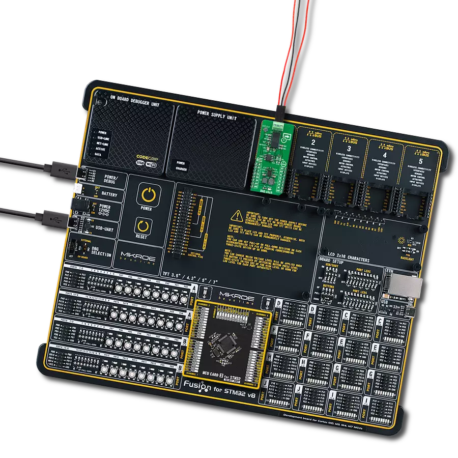
Development board
Fusion for STM32 v8 is a development board specially designed for the needs of rapid development of embedded applications. It supports a wide range of microcontrollers, such as different 32-bit ARM® Cortex®-M based MCUs from STMicroelectronics, regardless of their number of pins, and a broad set of unique functions, such as the first-ever embedded debugger/programmer over WiFi. The development board is well organized and designed so that the end-user has all the necessary elements, such as switches, buttons, indicators, connectors, and others, in one place. Thanks to innovative manufacturing technology, Fusion for STM32 v8 provides a fluid and immersive working experience, allowing
access anywhere and under any circumstances at any time. Each part of the Fusion for STM32 v8 development board contains the components necessary for the most efficient operation of the same board. An advanced integrated CODEGRIP programmer/debugger module offers many valuable programming/debugging options, including support for JTAG, SWD, and SWO Trace (Single Wire Output)), and seamless integration with the Mikroe software environment. Besides, it also includes a clean and regulated power supply module for the development board. It can use a wide range of external power sources, including a battery, an external 12V power supply, and a power source via the USB Type-C (USB-C) connector.
Communication options such as USB-UART, USB HOST/DEVICE, CAN (on the MCU card, if supported), and Ethernet is also included. In addition, it also has the well-established mikroBUS™ standard, a standardized socket for the MCU card (SiBRAIN standard), and two display options for the TFT board line of products and character-based LCD. Fusion for STM32 v8 is an integral part of the Mikroe ecosystem for rapid development. Natively supported by Mikroe software tools, it covers many aspects of prototyping and development thanks to a considerable number of different Click boards™ (over a thousand boards), the number of which is growing every day.

Microcontroller Overview
MCU Card / MCU
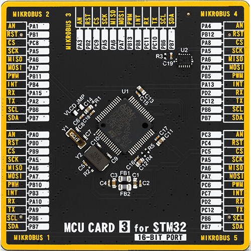
Type
8th Generation
Architecture
ARM Cortex-M0
MCU Memory (KB)
192
Silicon Vendor
STMicroelectronics
Pin count
64
RAM (Bytes)
20480
Used MCU Pins
mikroBUS™ mapper
Take a closer look
Click board™ Schematic

Step by step
Project assembly

Start by selecting your development board and Click board™. Begin with the Fusion for STM32 v8 as your development board.


Software Support
Library Description
This library contains API for DAQ Click driver.
Key functions:
daq_set_gainSet gain range.daq_read_dataReading adc data.daq_calculate_voltageConvert data from raw ADC to voltage.
Open Source
Code example
The complete application code and a ready-to-use project are available through the NECTO Studio Package Manager for direct installation in the NECTO Studio. The application code can also be found on the MIKROE GitHub account.
/*!
 * @file main.c
 * @brief DAQ Click example
 *
 * # Description
 * This example showcases ability of the device to read ADC
 * data and calculate voltage for set configuration.
 *
 * The demo application is composed of two sections :
 *
 * ## Application Init
 * Initialization of communication modules (SPI, UART) and
 * additional pins for controling device. Resets device and
 * then configures default configuration and sets read range
 * by setting gain to +-12V. In the end reads vendor and
 * device ID to confirm communication.
 *
 * ## Application Task
 * Reads ADC data and calculates voltage from it, every 0.3 seconds.
 *
 * @author Luka Filipovic
 *
 */

#include "board.h"
#include "log.h"
#include "daq.h"

static daq_t daq;
static log_t logger;

void application_init ( void )
{
    log_cfg_t log_cfg;  /**< Logger config object. */
    daq_cfg_t daq_cfg;  /**< Click config object. */

    /**
     * Logger initialization.
     * Default baud rate: 115200
     * Default log level: LOG_LEVEL_DEBUG
     * @note If USB_UART_RX and USB_UART_TX
     * are defined as HAL_PIN_NC, you will
     * need to define them manually for log to work.
     * See @b LOG_MAP_USB_UART macro definition for detailed explanation.
     */
    LOG_MAP_USB_UART( log_cfg );
    log_init( &logger, &log_cfg );
    log_info( &logger, " Application Init " );

    // Click initialization.
    daq_cfg_setup( &daq_cfg );
    DAQ_MAP_MIKROBUS( daq_cfg, MIKROBUS_1 );
    err_t init_flag  = daq_init( &daq, &daq_cfg );
    if ( SPI_MASTER_ERROR == init_flag )
    {
        log_error( &logger, " Application Init Error. " );
        log_info( &logger, " Please, run program again... " );

        for ( ; ; );
    }

    if ( daq_default_cfg ( &daq ) )
    {
        log_error( &logger, " Default configuration. " );
        log_info( &logger, " Please, run program again... " );

        for ( ; ; );
    }

    uint8_t id = 0;
    daq_generic_read( &daq, DAQ_REG_VENDOR_H, &id, 1 );
    log_printf( &logger, " > Vendor: \t0x%.2X", ( uint16_t )id );
    daq_generic_read( &daq, DAQ_REG_VENDOR_L, &id, 1 );
    log_printf( &logger, "%.2X\r\n", ( uint16_t )id );
    daq_generic_read( &daq, DAQ_REG_PRODUCT_ID_H, &id, 1 );
    log_printf( &logger, " > ID: \t\t0x%.2X", ( uint16_t )id );
    daq_generic_read( &daq, DAQ_REG_PRODUCT_ID_L, &id, 1 );
    log_printf( &logger, "%.2X\r\n", ( uint16_t )id );
    Delay_ms ( 1000 );

    log_info( &logger, " Application Task " );
}

void application_task ( void )
{
    int32_t adc_data = 0;
    float voltage = 0.0;
    daq_read_data( &daq, &adc_data );
    daq_calculate_voltage( &daq, adc_data, &voltage );

    log_printf( &logger, " > Data: %ld\r\n", adc_data );
    log_printf( &logger, " > Voltage: %.2f\r\n", voltage );
    log_printf( &logger, "***********************************\r\n" );
    Delay_ms ( 300 );
}

int main ( void )
{
    /* Do not remove this line or clock might not be set correctly. */
    #ifdef PREINIT_SUPPORTED
    preinit();
    #endif

    application_init( );

    for ( ; ; )
    {
        application_task( );
    }

    return 0;
}

// ------------------------------------------------------------------------ END
Additional Support
Resources
Category:ADC


