Track time with laser precision using AS6500 and MK64FX512VDC12
Sync up - time waits for none

Published May 27, 2023
Click board™
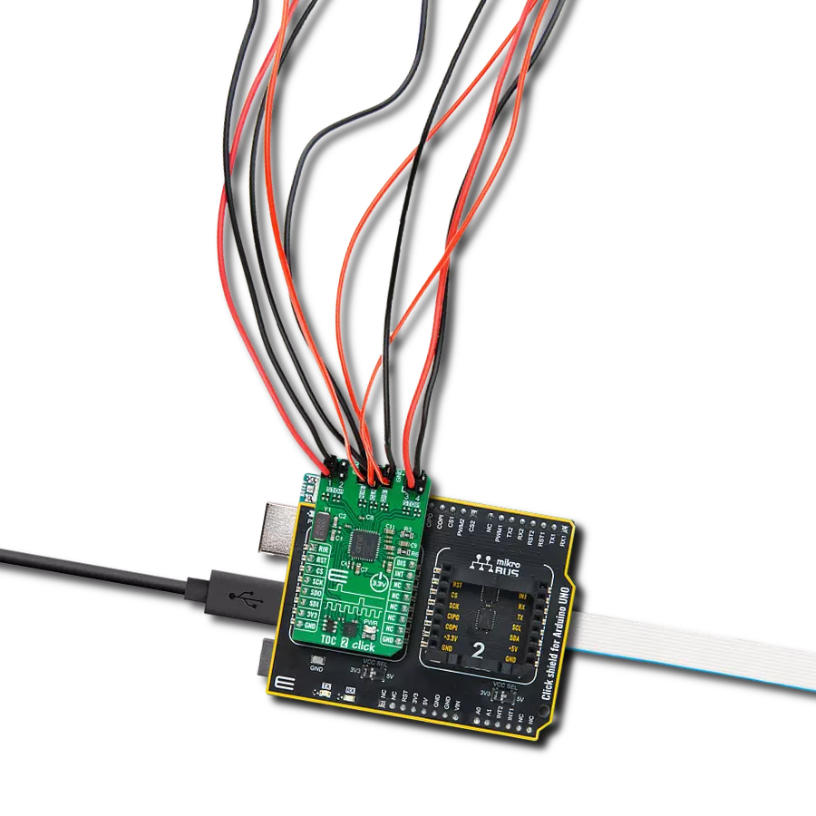
TDC 2 Click
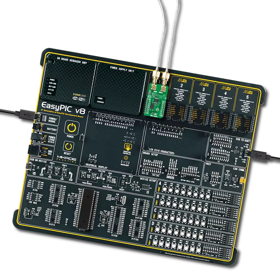
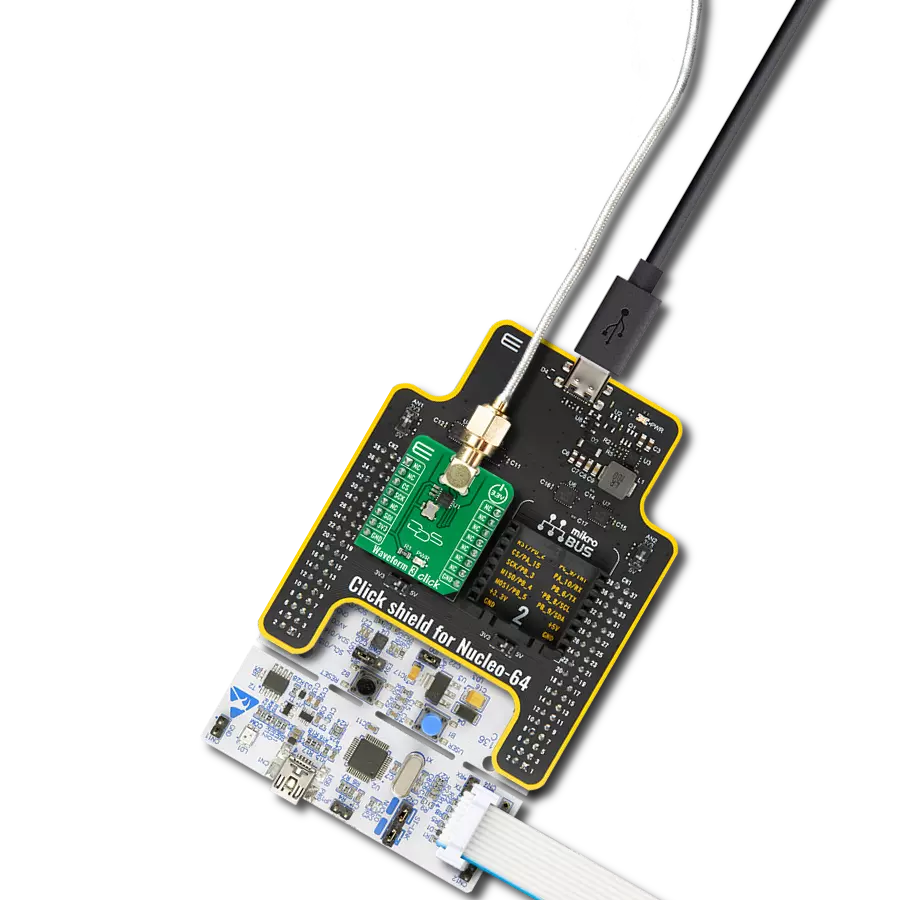
Dev. board
Fusion for ARM v8
Compiler
NECTO Studio
MCU
MK64FX512VDC12
Unleash the boundless possibilities of this high-performance time-to-digital converter today
A
A
Hardware Overview
How does it work?
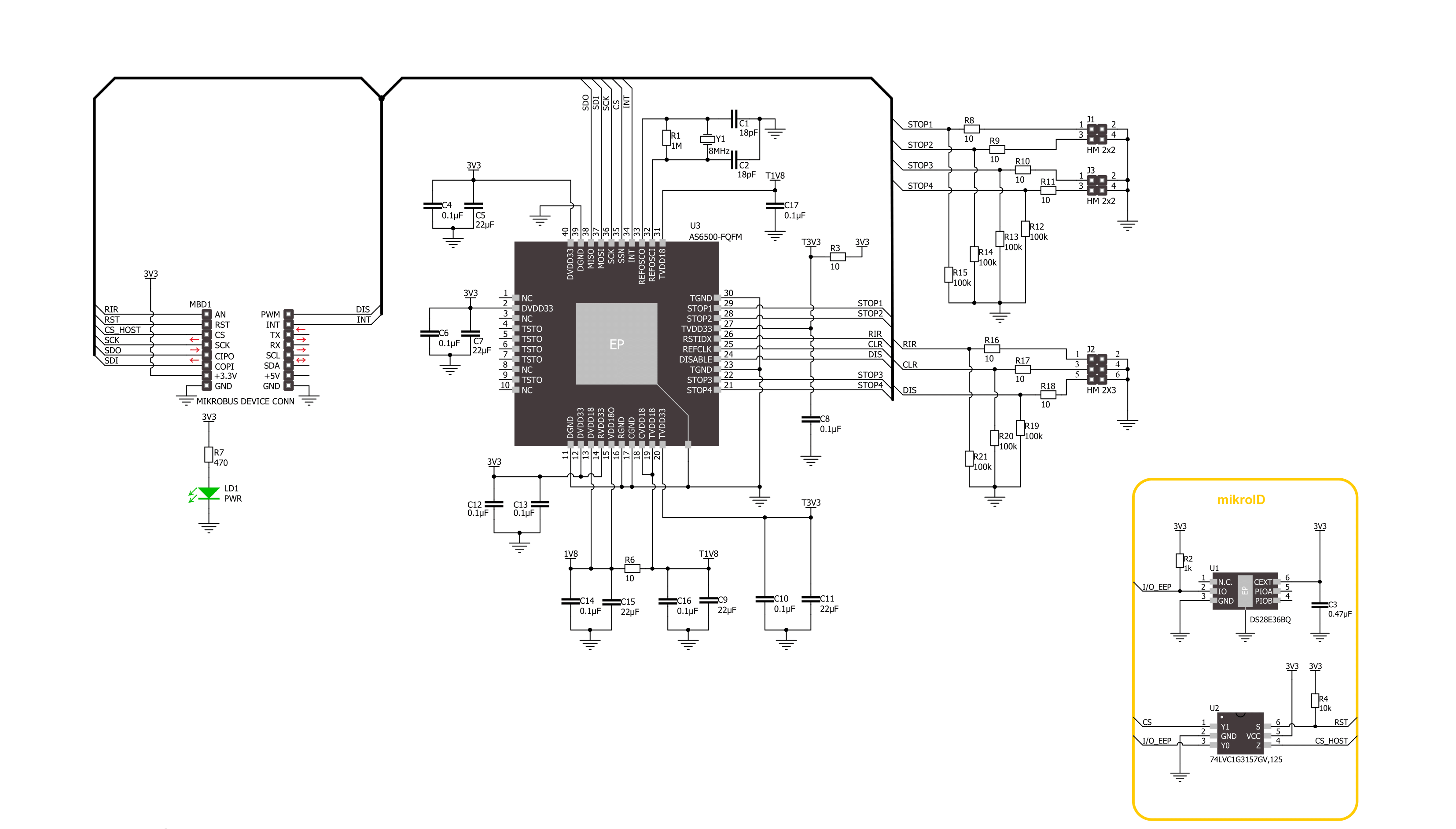
TDC 2 Click is based on the AS6500, a high-resolution time-to-digital converter from ScioSense, featuring CMOS inputs, high measurement performance, and high data throughput. The AS6500 can measure time intervals as low as 5ns with 10ps resolution on all four STOP channels at a sampling rate of up to 1.5Ms/s. It is characterized by high configuration flexibility, a wide measurement range from 0 to 16s, and simple data post-processing thanks to calibrated results. It calculates calibrated stop measurements referenced to the applied reference clock. This Click board™ is ideal for optical applications, including general-purpose laser distance measurement in 1D, 2D, and 3D, speed control, object recognition, time-of-flight spectroscopy, and many more. The positive edges of the stop signals, applied on the STOP terminals (1-4), are measured versus the preceding reference clock edge. The reference clock can be brought externally via the CLR
pin on the middle header terminal or from the onboard 8MHz quartz oscillator. This feature is selectable through software – register-setting. The reference clock represents the framework for all time measurements and serves as a universal time base. The TDC measures the clock pulses continuously as a time reference point for STOP pulses and an internal reference period. The measurement of the STOP events always refers to the preceding reference clock. The reference clock is counted continuously, and the actual count is assigned as a reference index to a STOP pulse. TDC 2 Click communicates with the host MCU through a standard SPI interface to read data and configure the frontend, supporting high clock speed up to 50MHz and the most common SPI mode, SPI Mode 1. SPI pins also use an interrupt pin that indicates to the host MCU that data are available and ready for processing. The AS6500 uses several more signals available on the
mikroBUS™ socket for successful time measurements. With the RIR pin, the internal counter for the reference index is set back to zero, simplifying the overview of the reference index in the output data stream. Next, setting the disable pin, marked as DIS, to a high logic state, the measurements on all four stops are disabled. On the other hand, the reference clock is not affected, and internal reference measurements are continued. Apart from the mikroBUS™ socket, these signals can also be found on the middle header, grouped with the reference clock pin. This Click board™ can only be operated with a 3.3V logic voltage level. The board must perform appropriate logic voltage level conversion before using MCUs with different logic levels. However, the Click board™ comes equipped with a library containing functions and an example code that can be used as a reference for further development.

Features overview
Development board
Fusion for ARM v8 is a development board specially designed for the needs of rapid development of embedded applications. It supports a wide range of microcontrollers, such as different ARM® Cortex®-M based MCUs regardless of their number of pins, and a broad set of unique functions, such as the first-ever embedded debugger/programmer over WiFi. The development board is well organized and designed so that the end-user has all the necessary elements, such as switches, buttons, indicators, connectors, and others, in one place. Thanks to innovative manufacturing technology, Fusion for ARM v8 provides a fluid and immersive working experience, allowing access anywhere and under any
circumstances at any time. Each part of the Fusion for ARM v8 development board contains the components necessary for the most efficient operation of the same board. An advanced integrated CODEGRIP programmer/debugger module offers many valuable programming/debugging options, including support for JTAG, SWD, and SWO Trace (Single Wire Output)), and seamless integration with the Mikroe software environment. Besides, it also includes a clean and regulated power supply module for the development board. It can use a wide range of external power sources, including a battery, an external 12V power supply, and a power source via the USB Type-C (USB-C) connector.
Communication options such as USB-UART, USB HOST/DEVICE, CAN (on the MCU card, if supported), and Ethernet is also included. In addition, it also has the well-established mikroBUS™ standard, a standardized socket for the MCU card (SiBRAIN standard), and two display options for the TFT board line of products and character-based LCD. Fusion for ARM v8 is an integral part of the Mikroe ecosystem for rapid development. Natively supported by Mikroe software tools, it covers many aspects of prototyping and development thanks to a considerable number of different Click boards™ (over a thousand boards), the number of which is growing every day.

Microcontroller Overview
MCU Card / MCU
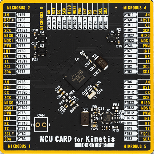
Type
8th Generation
Architecture
ARM Cortex-M4
MCU Memory (KB)
640
Silicon Vendor
NXP
Pin count
121
RAM (Bytes)
196608
Used MCU Pins
mikroBUS™ mapper
Take a closer look
Click board™ Schematic
Step by step
Project assembly

Start by selecting your development board and Click board™. Begin with the Fusion for ARM v8 as your development board.


Software Support
Library Description
This library contains API for TDC 2 Click driver.
Key functions:
tdc2_read_resultsTDC 2 results data reading function.tdc2_start_measuringTDC 2 start measuring function.tdc2_set_resolutionTDC 2 set resolution function.
Open Source
Code example
The complete application code and a ready-to-use project are available through the NECTO Studio Package Manager for direct installation in the NECTO Studio. The application code can also be found on the MIKROE GitHub account.
/*!
 * @file main.c
 * @brief TDC 2 Click example
 *
 * # Description
 * This library contains API for TDC 2 Click driver.
 * The library initializes and defines the SPI bus drivers to
 * write and read data from registers, as well as the default
 * configuration for a reading time between two STOP signals.
 *
 * The demo application is composed of two sections :
 *
 * ## Application Init
 * Initializes the driver after that resets the device and
 * performs default configuration and sets the device in read mode.

 *
 * ## Application Task
 * This example demonstrates the use of the TDC 2 Click board by
 * measuring the time between two STOP signals. This example is set up to
 * generate stop signals until FIFO fil's up which is indicated by interrupt pin going to low state.
 * After that FIFO buffer is completely emptied by reading, and that data is used to calculate
 * the time between STOP signals.
 *
 * @note
 * In order to test this example, you will need to connect STOP1 with the DIS pin. Disable pin is
 * disabled by software and it isn't going to affect the working state of the TDC 2 Click Bord.
 *
 * @author Stefan Ilic
 *
 */

#include "board.h"
#include "log.h"
#include "tdc2.h"

static tdc2_t tdc2;
static log_t logger;

/**
 * @brief Dev generate stop signal function.
 * @details This function generates the stop signal by toggling DIS pin.
 * @param[out] cfg : Click configuration structure.
 * See #tdc2_cfg_t object definition for detailed explanation.
 * @return Nothing.
 * @note DIS pin ( Disable STOP channels) is disabled by software and isn't affecting the example.
 */
void dev_generate_stop( tdc2_t *ctx );

void application_init ( void )
{
    log_cfg_t log_cfg;  /**< Logger config object. */
    tdc2_cfg_t tdc2_cfg;  /**< Click config object. */

    /**
     * Logger initialization.
     * Default baud rate: 115200
     * Default log level: LOG_LEVEL_DEBUG
     * @note If USB_UART_RX and USB_UART_TX
     * are defined as HAL_PIN_NC, you will
     * need to define them manually for log to work.
     * See @b LOG_MAP_USB_UART macro definition for detailed explanation.
     */
    LOG_MAP_USB_UART( log_cfg );
    log_init( &logger, &log_cfg );
    log_info( &logger, " Application Init " );

    // Click initialization.
    tdc2_cfg_setup( &tdc2_cfg );
    TDC2_MAP_MIKROBUS( tdc2_cfg, MIKROBUS_1 );
    if ( SPI_MASTER_ERROR == tdc2_init( &tdc2, &tdc2_cfg ) )
    {
        log_error( &logger, " Communication init." );
        for ( ; ; );
    }

    if ( TDC2_ERROR == tdc2_default_cfg ( &tdc2 ) )
    {
        log_error( &logger, " Default configuration." );
        for ( ; ; );
    }

    tdc2_start_measuring ( &tdc2 );
    log_info( &logger, " Application Task " );
}

void application_task ( void )
{
    uint32_t reference_index [ 18 ] = { 0 };
    uint32_t stop_result [ 18 ] = { 0 };
    uint8_t cnt = 0;

    tdc2_reset_index( &tdc2 );
    Delay_ms ( 10 );

    while ( tdc2_get_int_state( &tdc2 ) == 1 )
    {
        dev_generate_stop( &tdc2 );
        Delay_ms ( 100 );
    }

    while ( tdc2_get_int_state( &tdc2 ) == 0 )
    {
        tdc2_read_results( &tdc2, TDC2_REG_INDEX_CH1_BYTE3, &reference_index[ cnt ], &stop_result[ cnt ] );

        log_printf( &logger, "CH1: Reference Index[%d]: %lu, Stop Result[%d]: %lu \r\n", ( uint16_t ) cnt,
                    reference_index[ cnt ], ( uint16_t ) cnt, stop_result[ cnt ] );
        Delay_ms ( 10 );

        if ( cnt )
        {
            uint32_t time = 0;
            tdc2_get_time_between_stops ( &tdc2, stop_result[ cnt - 1 ], reference_index[ cnt - 1 ],
                                          stop_result[ cnt ], reference_index[ cnt ], &time );
            log_printf( &logger, "Time between STOP %d and STOP %d is %lu ms \r\n",
                        ( uint16_t ) ( cnt - 1 ), ( uint16_t ) cnt, time / TDC2_uS_TO_mS );
            Delay_ms ( 10 );
        }
        cnt++;
    }
    log_printf( &logger, "---------------------------------------------- \r\n" );
}

int main ( void )
{
    /* Do not remove this line or clock might not be set correctly. */
    #ifdef PREINIT_SUPPORTED
    preinit();
    #endif

    application_init( );

    for ( ; ; )
    {
        application_task( );
    }

    return 0;
}

void dev_generate_stop( tdc2_t *ctx )
{
    digital_out_high( &ctx->dis );
    Delay_ms ( 1 );
    digital_out_low( &ctx->dis );
}

// ------------------------------------------------------------------------ END
Additional Support
Resources
Category:Clock generator