Master the art of precise timing with CS2200-CP and PIC32MZ2048EFH144
Clock frequency synthesizer

Published May 27, 2023
Click board™
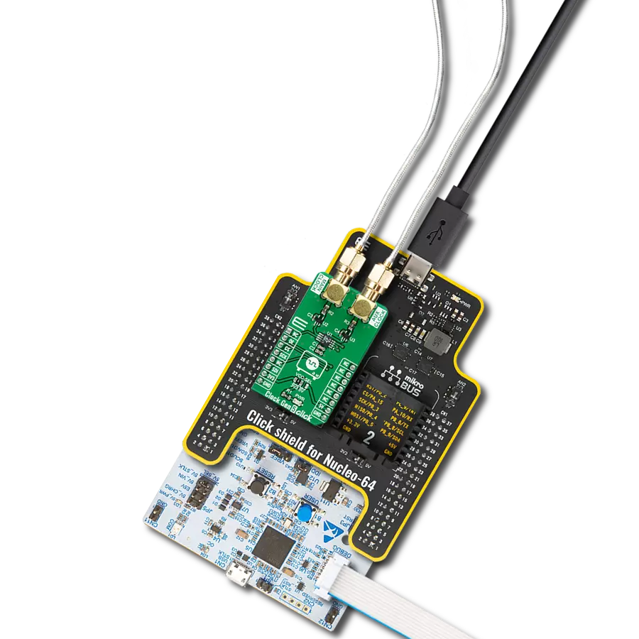
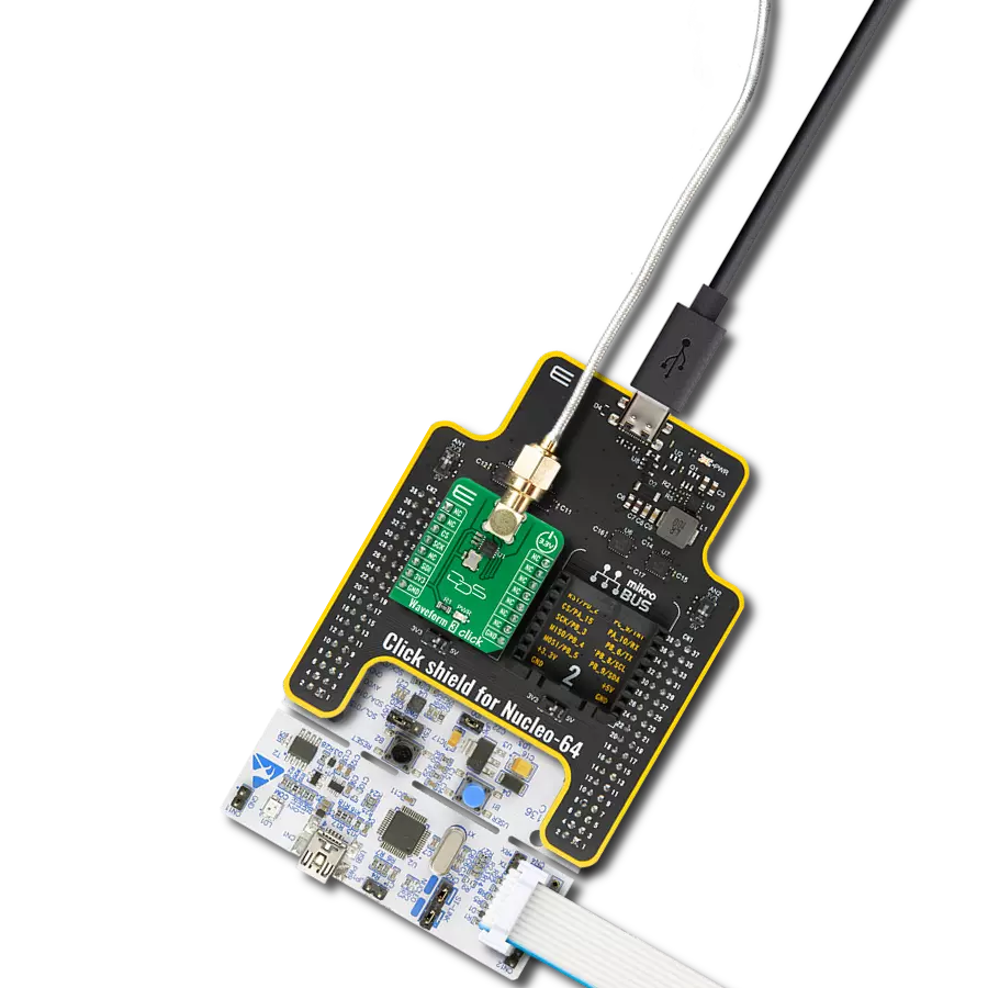
Clock Gen 4 Click
Dev. board
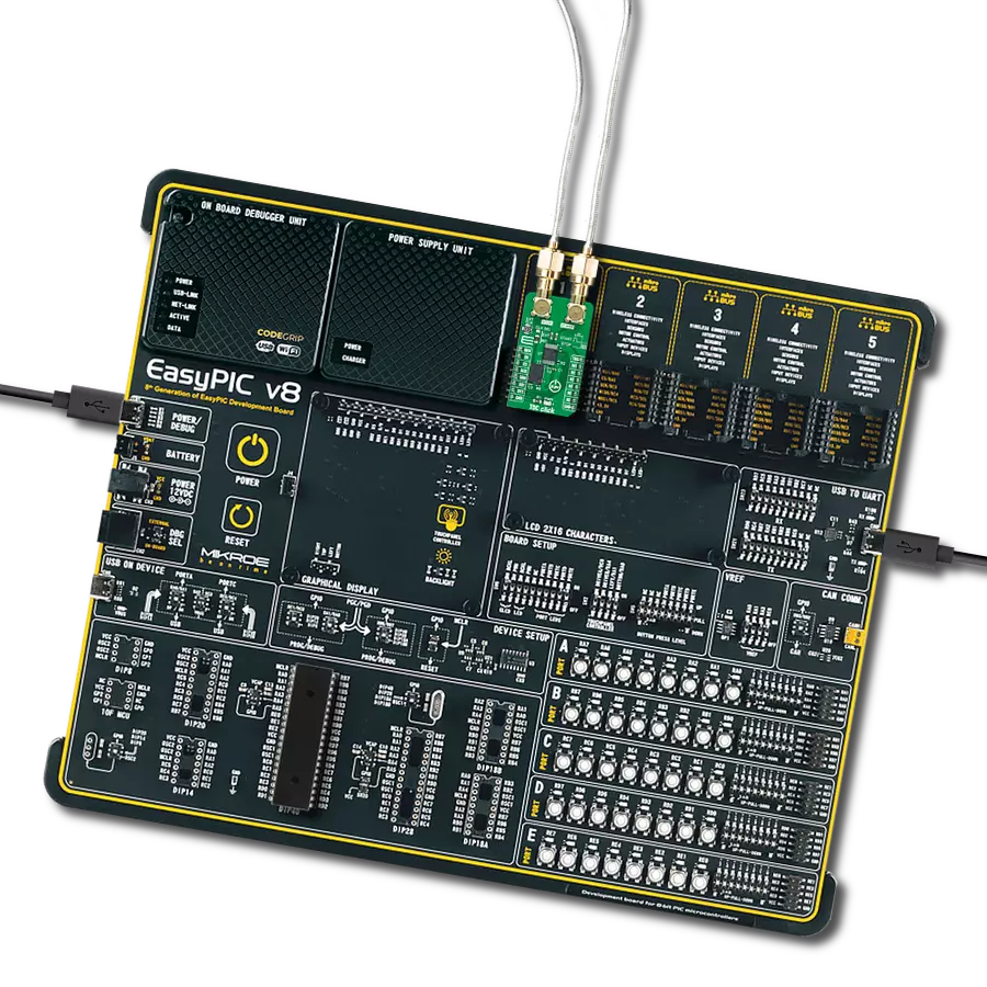
Fusion for PIC32 v8
Compiler
NECTO Studio
MCU
PIC32MZ2048EFH144
Integrate an advanced clock generator into your solution and witness the transformative impact on timing control
A
A
Hardware Overview
How does it work?
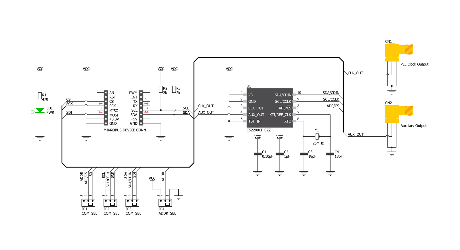
Clock Gen 4 Click is based on the CS2200-CP, an analog PLL architecture comprised of a Delta-Sigma fractional-N frequency synthesizer from Cirrus Logic. The Delta-Sigma fractional-N frequency synthesizer has a high resolution for Input/Output clock ratios, low phase noise, a wide range of output frequencies, and the ability to tune to a new frequency quickly. This synthesizer multiplies the timing reference clock by the value of N to generate a stable and low-jitter PLL clock on the connector labeled PLL Clock. This Click board™ also has another connector marked as AUX Clock that outputs a buffered version of one of the input/output clocks or a status signal, depending on register configuration. The analog PLL-based frequency synthesizer uses a low-jitter timing reference clock
as a time and phase reference for the internal voltage-controlled oscillator (VCO). The phase comparator compares the fractional-N divided clock with the original timing reference and generates a control signal filtered by the internal loop filter to generate the VCO’s control voltage that sets its output frequency. The Delta-Sigma modulator modulates the loop integer divide ratio to get the desired fractional ratio between the reference clock and the VCO output. This allows fast lock times for various output frequencies without external filter components. Clock Gen 4 Click provides the possibility of using both I2C and SPI interfaces with a maximum frequency of 100kHz for I2C and 6MHz for SPI communication. The selection can be performed by positioning SMD jumpers labeled
COMM SEL to an appropriate position. Note that all the jumpers must be placed on the same side, or the Click board™ may become unresponsive. While the I2C interface is selected, the CS2200-CP allows the choice of the least significant bit (LSB) of its I2C slave address. This can be done by using the SMD jumper labeled as ADDR SEL. This Click board™ can only be operated with a 3.3V logic voltage level. The board must perform appropriate logic voltage level conversion before using MCUs with different logic levels. However, the Click board™ comes equipped with a library containing functions and an example code that can be used as a reference for further development.

Features overview
Development board
Fusion for PIC32 v8 is a development board specially designed for the needs of rapid development of embedded applications. It supports a wide range of Microchip's PIC32 microcontrollers regardless of their number of pins and a broad set of unique functions, such as the first-ever embedded debugger/programmer over WiFi. The development board is well organized and designed so that the end-user has all the necessary elements, such as switches, buttons, indicators, connectors, and others, in one place. Thanks to innovative manufacturing technology, Fusion for PIC32 v8 provides a fluid and immersive working experience, allowing access anywhere and under any circumstances at any time. Each part of the
Fusion for PIC32 v8 development board contains the components necessary for the most efficient operation of the same board. In addition to the advanced integrated CODEGRIP programmer/debugger module, which offers many valuable programming/debugging options and seamless integration with the Mikroe software environment, the board also includes a clean and regulated power supply module for the development board. It can use a wide range of external power sources, including a battery, an external 12V power supply, and a power source via the USB Type-C (USB-C) connector. Communication options such as USB-UART, USB HOST/DEVICE, CAN (on the MCU card, if
supported), and Ethernet is also included. In addition, it also has the well-established mikroBUS™ standard, a standardized socket for the MCU card (SiBRAIN standard), and two display options for the TFT board line of products and character-based LCD. Fusion for PIC32 v8 is an integral part of the Mikroe ecosystem for rapid development. Natively supported by Mikroe software tools, it covers many aspects of prototyping and development thanks to a considerable number of different Click boards™ (over a thousand boards), the number of which is growing every day.

Microcontroller Overview
MCU Card / MCU
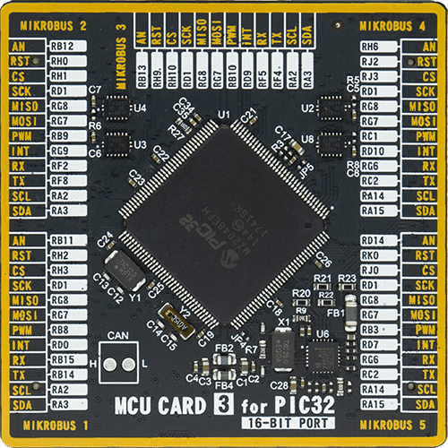
Type
8th Generation
Architecture
PIC32
MCU Memory (KB)
2048
Silicon Vendor
Microchip
Pin count
144
RAM (Bytes)
524288
Used MCU Pins
mikroBUS™ mapper
Take a closer look
Click board™ Schematic
Step by step
Project assembly

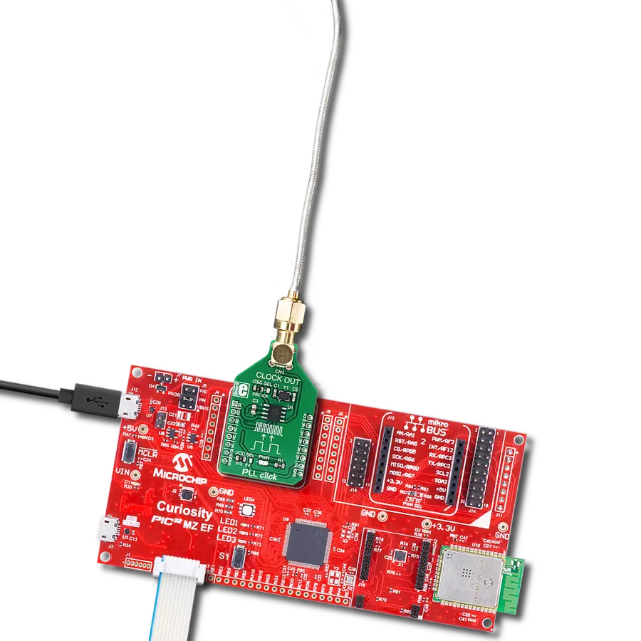
Start by selecting your development board and Click board™. Begin with the Fusion for PIC32 v8 as your development board.


Software Support
Library Description
This library contains API for Clock Gen 4 Click driver.
Key functions:
void clockgen4_dev_ctl ( uint8_t dev_ctl );- Function is used to write to Device Control register in order to apply settings.void clockgen4_dev_cfg ( uint8_t dev_cfg );- Function is used to write to Device Configuration 1 register in order to apply settings.uint32_t clockgen4_set_ratio ( float ratio );- Function is used to set the ratio between the output signal and the input clock.
Open Source
Code example
The complete application code and a ready-to-use project are available through the NECTO Studio Package Manager for direct installation in the NECTO Studio. The application code can also be found on the MIKROE GitHub account.
/*!
 * @file main.c
 * @brief ClockGen4 Click example
 *
 * # Description
 * This example demonstrates the use of Clock Gen 4 Click which is based on CS2200-CP for changing the channel clock. The CS2200-CP is an extremely
 * versatile system clocking device that utilizes a programmable phase lock loop. The CS2200-CP is based on an analog PLL architecture and this
 * architecture allows for frequency synthesis and clock generation from a stable reference clock. The CS2200-CP supports both I²C and SPI for full software control.
 *
 * The demo application is composed of two sections :
 *
 * ## Application Init
 * Initializes I2C and SPI, sets CS pin as output and starts to write log, applies default settings and adjusted ratio to obtain a frequency.
 *
 * ## Application Task
 * Clock Gen 4 Click is used in this example to generate and change the clock on the output channel.
 *
 * @author Jelena Milosavljevic
 *
 */

#include "board.h"
#include "log.h"
#include "clockgen4.h"

static clockgen4_t clockgen4;
static log_t logger;

uint8_t com_itfc = 0;

void application_init ( void ){
    log_cfg_t log_cfg;                     /**< Logger config object. */
    clockgen4_cfg_t clockgen4_cfg;         /**< Click config object. */

    /**
     * Logger initialization.
     * Default baud rate: 115200
     * Default log level: LOG_LEVEL_DEBUG
     * @note If USB_UART_RX and USB_UART_TX
     * are defined as HAL_PIN_NC, you will
     * need to define them manually for log to work.
     * See @b LOG_MAP_USB_UART macro definition for detailed explanation.
     */
    LOG_MAP_USB_UART( log_cfg );
    log_init( &logger, &log_cfg );
    log_info( &logger, " Application Init " );

    Delay_ms ( 100 );
    log_printf( &logger, "---------------------" );
    log_printf( &logger, "  Clock Gen 4 Click  " );
    log_printf( &logger, "---------------------" );

    // Click initialization.
    clockgen4_cfg_setup( &clockgen4_cfg );
    CLOCKGEN4_MAP_MIKROBUS( clockgen4_cfg, MIKROBUS_1 );
    err_t init_flag  = clockgen4_init( &clockgen4, &clockgen4_cfg );
    if ( ( I2C_MASTER_ERROR == init_flag ) || ( SPI_MASTER_ERROR == init_flag ) ) {
        log_error( &logger, " Application Init Error. " );
        log_info( &logger, " Please, run program again... " );

        for ( ; ; );
    }

    clockgen4_default_cfg ( &clockgen4 );
    log_info( &logger, " Application Task " );
    Delay_ms ( 100 );
}

void application_task ( void ){
    clockgen4_dev_ctl ( &clockgen4, CLOCKGEN4_AUX_OUT_DIS | CLOCKGEN4_CLK_OUT_EN );
    log_printf( &logger, "  PLL Clock          \r\n" );
    log_printf( &logger, "  output enabled!    \r\n" );
    log_printf( &logger, "---------------------\r\n" );
    Delay_ms ( 1000 );

    clockgen4_dev_ctl ( &clockgen4, CLOCKGEN4_AUX_OUT_EN | CLOCKGEN4_CLK_OUT_DIS );
    log_printf( &logger, "  AUX Clock          \r\n" );
    log_printf( &logger, "  output enabled!    \r\n" );
    log_printf( &logger, "---------------------\r\n" );
    Delay_ms ( 1000 );
}

int main ( void )
{
    /* Do not remove this line or clock might not be set correctly. */
    #ifdef PREINIT_SUPPORTED
    preinit();
    #endif

    application_init( );

    for ( ; ; )
    {
        application_task( );
    }

    return 0;
}

// ------------------------------------------------------------------------ END
Additional Support
Resources
Category:Clock generator