Convert digital signals into tangible analog outputs using DAC53401 and MK64FX512VDC12
Redefine data with our DAC symphony!

Published Aug 19, 2023
Click board™
DAC 10 Click
Dev. board
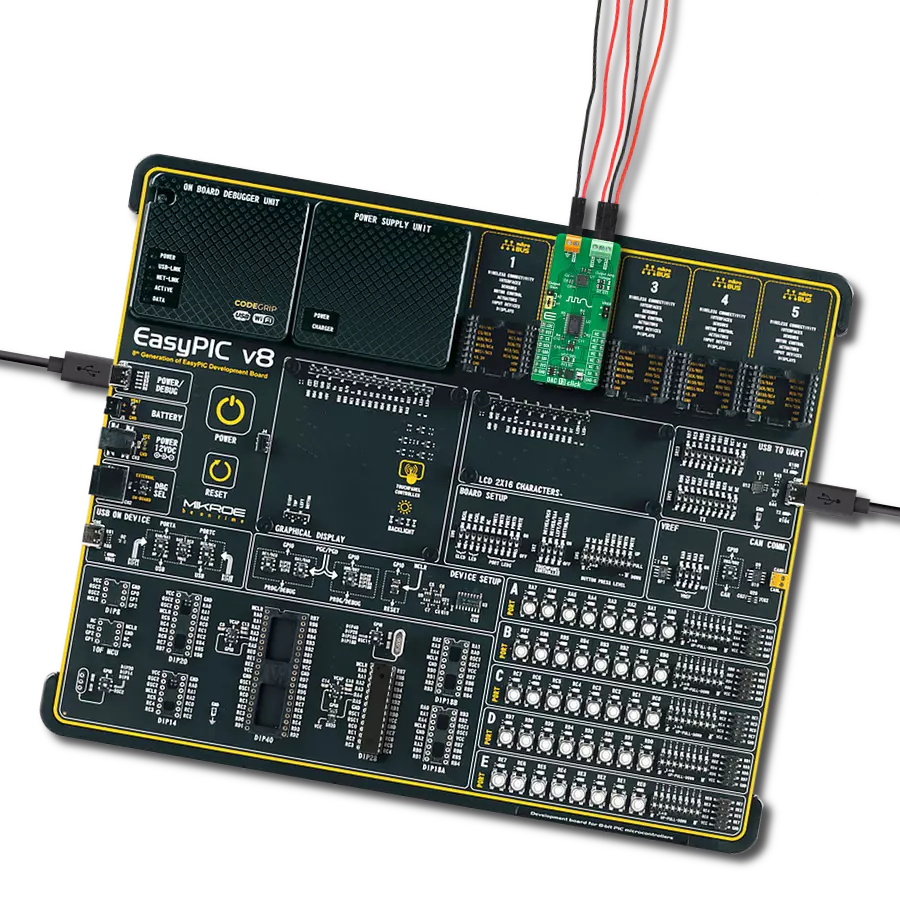
Fusion for Kinetis v8
Compiler
NECTO Studio
MCU
MK64FX512VDC12
Our DAC solution empowers data to transcend the digital realm, converting it into actionable analog outputs and fostering effective communication and control across many applications
A
A
Hardware Overview
How does it work?
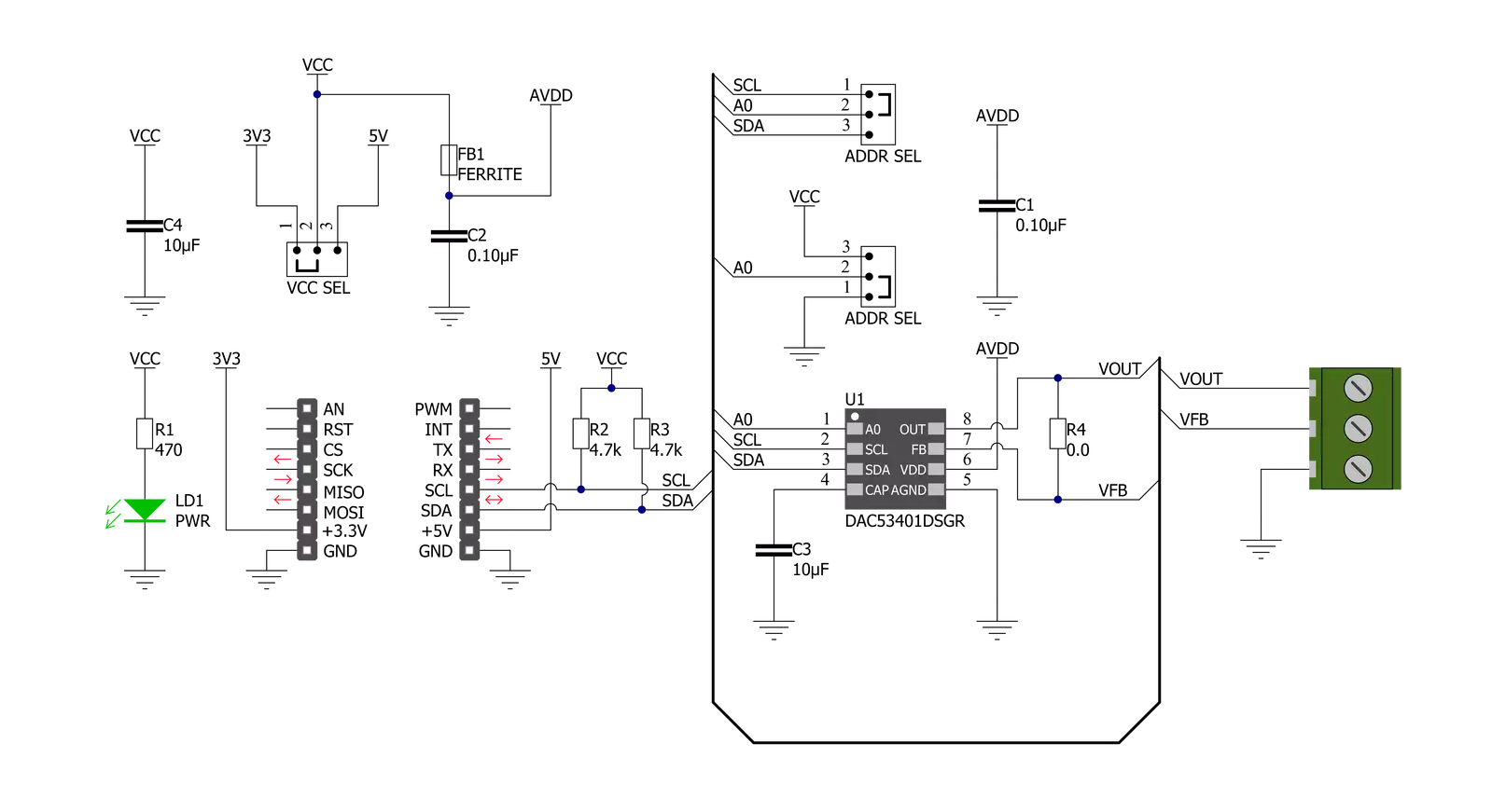
DAC 10 Click is based on the DAC53401, a 10-bit voltage-output smart digital-to-analog converter from Texas Instruments. This device consumes extremely low power and has a nonvolatile memory (NVM), an internal reference, and an I2C serial interface. It also has a power-on-reset circuit that ensures all the registers start with default or user-programmed settings using NVM. It operates with either an internal reference or the power supply as a reference and provides full-scale output from 0V to 5.5V. The DAC53401 includes digital slew rate control and supports basic signal generation such as square, ramp, and sawtooth waveforms. It also can generate pulse-width modulation (PWM) output with the
combination of the triangular or sawtooth waveform and the VFB terminal. The DAC53401 is also called a smart DAC device because of its advanced integrated features. This smart DAC's force-sense output, PWM output, and NVM capabilities enable system performance and control without using the software. These features allow DAC53401 to go beyond a conventional DAC's limitations that depend on a processor to function. DAC 10 Click communicates with MCU using the standard I2C 2-Wire interface to read data and configure settings, supporting Standard Mode operation with a clock frequency up to 100kHz, Fast Mode up to 400kHz, and Fast Mode Plus up to 1MHz. Besides, it also allows the
choice of the three least significant bits of its I2C slave address by positioning the SMD jumper labeled as ADDR SEL to an appropriate position marked as 0, 1, SCL, and SDA, providing the user with a choice of 4 I2C Slave addresses. This Click board™ can operate with either 3.3V or 5V logic voltage levels selected via the VCC SEL jumper. This way, both 3.3V and 5V capable MCUs can use the communication lines properly. Also, this Click board™ comes equipped with a library containing easy-to-use functions and an example code that can be used, as a reference, for further development.

Features overview
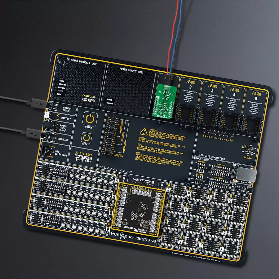
Development board
Fusion for KINETIS v8 is a development board specially designed for the needs of rapid development of embedded applications. It supports a wide range of microcontrollers, such as different 32-bit ARM® Cortex®-M based MCUs from NXP Semiconductor, regardless of their number of pins, and a broad set of unique functions, such as the first-ever embedded debugger/programmer over a WiFi network. The development board is well organized and designed so that the end-user has all the necessary elements, such as switches, buttons, indicators, connectors, and others, in one place. Thanks to innovative manufacturing technology, Fusion for KINETIS v8 provides a fluid and immersive working experience, allowing
access anywhere and under any circumstances at any time. Each part of the Fusion for KINETIS v8 development board contains the components necessary for the most efficient operation of the same board. An advanced integrated CODEGRIP programmer/debugger module offers many valuable programming/debugging options, including support for JTAG, SWD, and SWO Trace (Single Wire Output)), and seamless integration with the Mikroe software environment. Besides, it also includes a clean and regulated power supply module for the development board. It can use a wide range of external power sources, including a battery, an external 12V power supply, and a power source via the USB Type-C (USB-C) connector.
Communication options such as USB-UART, USB HOST/DEVICE, CAN (on the MCU card, if supported), and Ethernet is also included. In addition, it also has the well-established mikroBUS™ standard, a standardized socket for the MCU card (SiBRAIN standard), and two display options for the TFT board line of products and character-based LCD. Fusion for KINETIS v8 is an integral part of the Mikroe ecosystem for rapid development. Natively supported by Mikroe software tools, it covers many aspects of prototyping and development thanks to a considerable number of different Click boards™ (over a thousand boards), the number of which is growing every day.

Microcontroller Overview
MCU Card / MCU
Type
8th Generation
Architecture
ARM Cortex-M4
MCU Memory (KB)
640
Silicon Vendor
NXP
Pin count
121
RAM (Bytes)
196608
Used MCU Pins
mikroBUS™ mapper
Take a closer look
Click board™ Schematic
Step by step
Project assembly

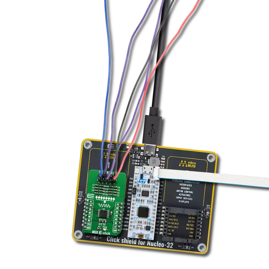
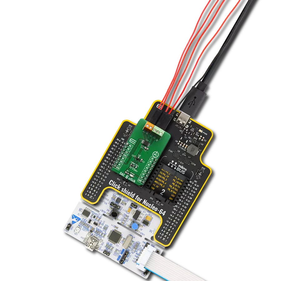
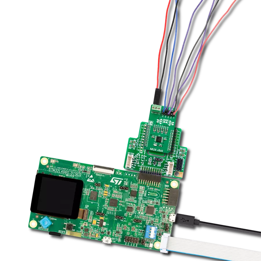
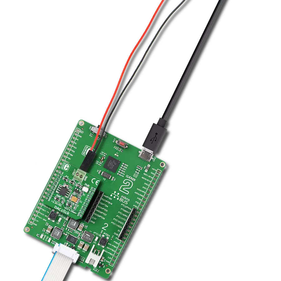
Start by selecting your development board and Click board™. Begin with the Fusion for Kinetis v8 as your development board.


Software Support
Library Description
This library contains API for DAC 10 Click driver.
Key functions:
dac10_check_device_id- This function checks the communication by reading and verifying the device IDdac10_enable_dac- This function enables the DAC outputdac10_set_output_voltage- This function sets the output voltage depending on the vref value
Open Source
Code example
The complete application code and a ready-to-use project are available through the NECTO Studio Package Manager for direct installation in the NECTO Studio. The application code can also be found on the MIKROE GitHub account.
/*!
 * @file main.c
 * @brief DAC10 Click example
 *
 * # Description
 * This example demonstrates the use of DAC 10 Click board.
 *
 * The demo application is composed of two sections :
 *
 * ## Application Init
 * Initializes the driver, checks the communication by reading and verifying the device ID,
 * and enables the DAC output.
 *
 * ## Application Task
 * Changes the output voltage every 2 seconds and logs the voltage value on the USB UART.
 * It will go through the entire voltage range taking into account the number of steps
 * which is defined below.
 *
 * @note
 * Measure the voltage at VCC_SEL jumper and adjust the reference voltage value below for better accuracy.
 *
 * @author Stefan Filipovic
 *
 */

#include "board.h"
#include "log.h"
#include "dac10.h"

#define REFERENCE_VOLTAGE  3.3 // The reference voltage defined by the VCC_SEL on-board jumper.
#define NUMBER_OF_STEPS    20  // The number of steps by which we will divide the entire voltage range.

static dac10_t dac10;
static log_t logger;

void application_init ( void )
{
    log_cfg_t log_cfg;  /**< Logger config object. */
    dac10_cfg_t dac10_cfg;  /**< Click config object. */

    /**
     * Logger initialization.
     * Default baud rate: 115200
     * Default log level: LOG_LEVEL_DEBUG
     * @note If USB_UART_RX and USB_UART_TX
     * are defined as HAL_PIN_NC, you will
     * need to define them manually for log to work.
     * See @b LOG_MAP_USB_UART macro definition for detailed explanation.
     */
    LOG_MAP_USB_UART( log_cfg );
    log_init( &logger, &log_cfg );
    Delay_ms ( 100 );
    log_info( &logger, " Application Init " );

    // Click initialization.
    dac10_cfg_setup( &dac10_cfg );
    DAC10_MAP_MIKROBUS( dac10_cfg, MIKROBUS_1 );
    err_t init_flag = dac10_init( &dac10, &dac10_cfg );
    if ( I2C_MASTER_ERROR == init_flag )
    {
        log_error( &logger, " Application Init Error. " );
        log_info( &logger, " Please, run program again... " );

        for ( ; ; );
    }

    if ( DAC10_ERROR == dac10_check_device_id ( &dac10 ) )
    {
        log_error( &logger, " Check Device ID Error. " );
        log_info( &logger, " Please, run program again... " );

        for ( ; ; );
    }

    dac10_enable_dac( &dac10 );
    Delay_ms ( 100 );
    log_info( &logger, " Application Task " );
}

void application_task ( void )
{
    float step = REFERENCE_VOLTAGE / NUMBER_OF_STEPS;
    float output_voltage = step;
    uint8_t cnt = 0;
    while ( cnt < NUMBER_OF_STEPS )
    {
        dac10_set_output_voltage ( &dac10, REFERENCE_VOLTAGE, output_voltage );
        log_printf( &logger, " DAC output voltage set to %.2f V\r\n", output_voltage );
        output_voltage += step;
        cnt++;
        Delay_ms ( 1000 );
        Delay_ms ( 1000 );
    }
}

int main ( void )
{
    /* Do not remove this line or clock might not be set correctly. */
    #ifdef PREINIT_SUPPORTED
    preinit();
    #endif

    application_init( );

    for ( ; ; )
    {
        application_task( );
    }

    return 0;
}

// ------------------------------------------------------------------------ END