Convert frequency input into voltage output with exceptional accuracy using VFC32KU and STM32F373RC
Transforming waves into voltage: The future of signal analysis

Published Dec 09, 2023
Click board™
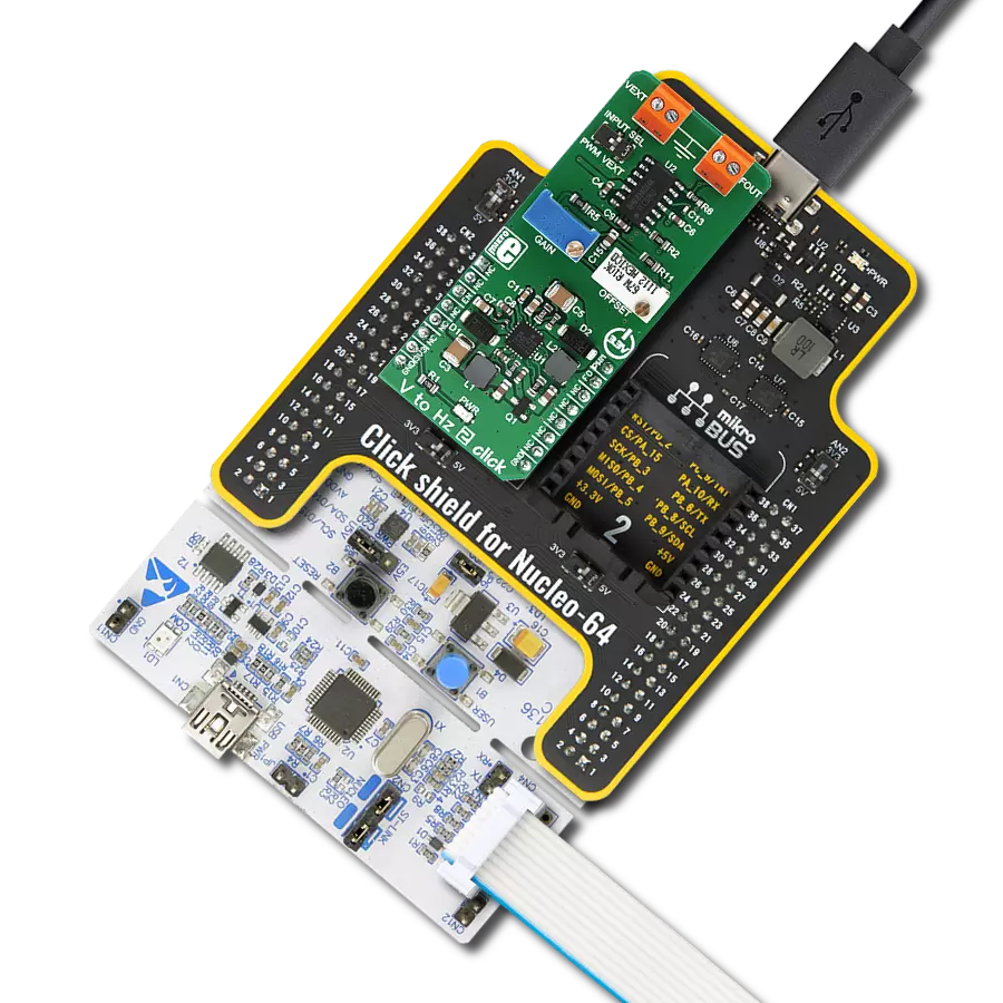
Hz To V 2 Click
Dev. board
Fusion for STM32 v8
Compiler
NECTO Studio
MCU
STM32F373RC
Translate frequency data into voltage signals, setting a new standard for signal analysis and control
A
A
Hardware Overview
How does it work?
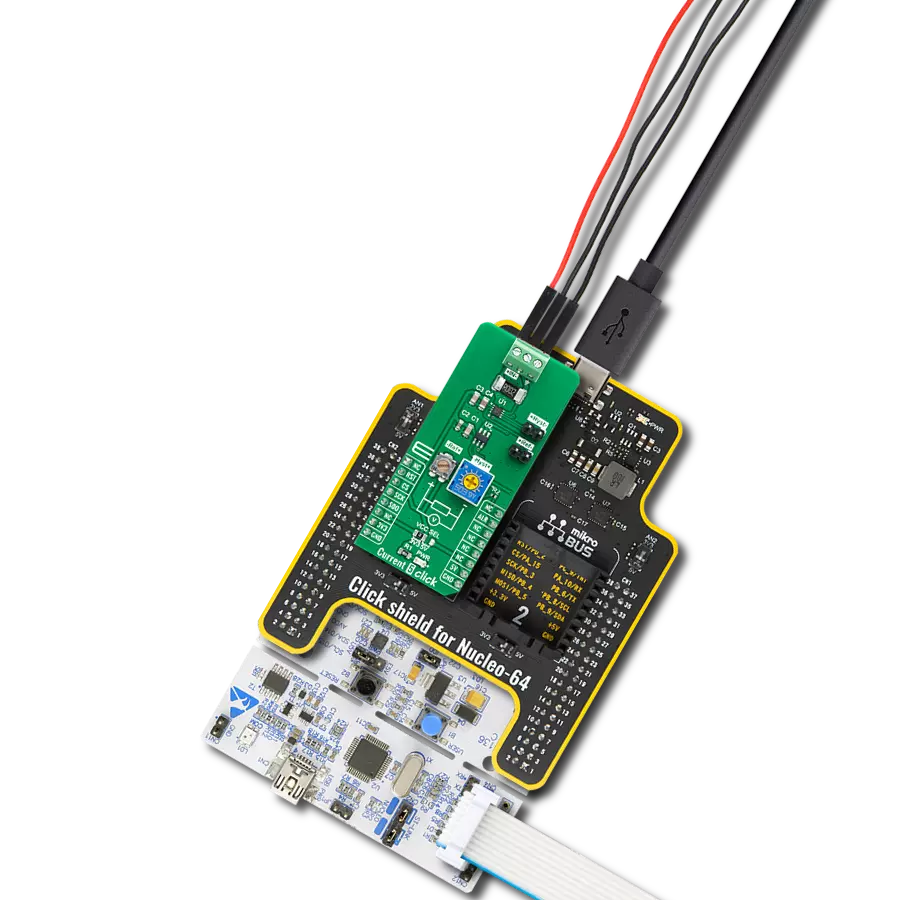
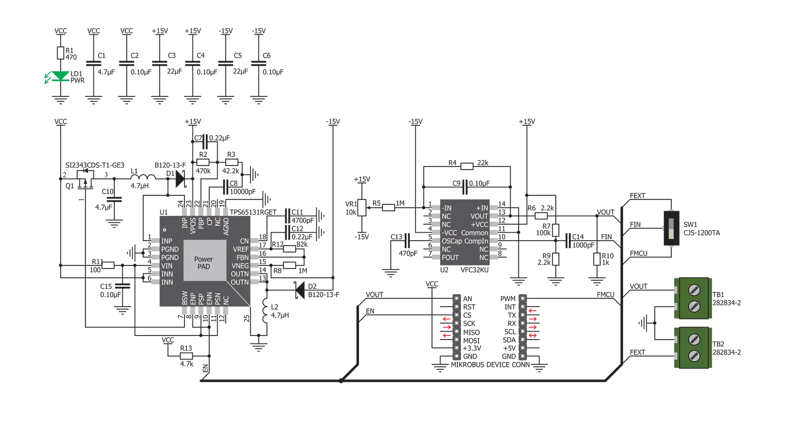
Hz to V 2 Click is based on the VFC32KU, a voltage-to-frequency and frequency-to-voltage converter from Texas Instruments. It accepts a signal with the frequency within a range between 200Hz and 120kHz on the input and generates DC voltage with the level corresponding to the input frequency, ranging from 0V to 10V, with a highly linear response. The output DC voltage level is further scaled down by the voltage divider on the VFC32KU output, in order to achieve levels acceptable by the MCU. This makes the DC voltage output suitable for sampling, or further processing by the host MCU. The input signal within the specified frequency range can be applied to either the PWM pin of the mikroBUS™ labeled as FIN on this Click board™ or to the external signal input terminal labeled as FEXT. This signal is AC coupled by a 1nF capacitor, meaning
that no DC component will be affecting the connected source. The signal input source can be selected by the onboard switch, labeled as INPUT SEL. A DC voltage output ranging up to 3.3V is available both on the AN pin of the mikroBUS™ labeled as the VO, and the output terminal - labeled as the VOUT on this Click board™. An onboard high-precision OFFSET potentiometer is used to fine-tune the output of the Click board™. It can be calibrated by using the offset potentiometer, by introducing a signal of a known frequency to either FEXT input terminal or the PWM input pin. An offset trimming procedure should be executed before the first use of the Click board™, since even slight variations in the components tolerances could affect the value at the output. It is recommended to correct the offset after longer time intervals, to compensate
for the aging of the passive components on the Click board™. The VFC32KU IC requires a dual power supply with ±15V. Therefore, this Click board™ utilizes another IC in order to provide the required voltages. It uses the TPS65131, a positive and negative output DC/DC Converter IC, also from Texas Instruments. This DC/DC converter has already been used in Boost-INV 2 click, so it was tested "on the field" for this purpose. Providing well-stabilized output with the plenty of power headroom, it is a perfect solution for the HZ to V 2 click, also. To enable the conversion circuitry, the EN pin of the TPS65131 boost converter should be pulled to a HIGH logic level. This will activate the boost converter and provide the required power for the VFC32KU IC. This pin is routed to the mikroBUS™ CS pin and it is labeled as EN.

Features overview
Development board
Fusion for STM32 v8 is a development board specially designed for the needs of rapid development of embedded applications. It supports a wide range of microcontrollers, such as different 32-bit ARM® Cortex®-M based MCUs from STMicroelectronics, regardless of their number of pins, and a broad set of unique functions, such as the first-ever embedded debugger/programmer over WiFi. The development board is well organized and designed so that the end-user has all the necessary elements, such as switches, buttons, indicators, connectors, and others, in one place. Thanks to innovative manufacturing technology, Fusion for STM32 v8 provides a fluid and immersive working experience, allowing
access anywhere and under any circumstances at any time. Each part of the Fusion for STM32 v8 development board contains the components necessary for the most efficient operation of the same board. An advanced integrated CODEGRIP programmer/debugger module offers many valuable programming/debugging options, including support for JTAG, SWD, and SWO Trace (Single Wire Output)), and seamless integration with the Mikroe software environment. Besides, it also includes a clean and regulated power supply module for the development board. It can use a wide range of external power sources, including a battery, an external 12V power supply, and a power source via the USB Type-C (USB-C) connector.
Communication options such as USB-UART, USB HOST/DEVICE, CAN (on the MCU card, if supported), and Ethernet is also included. In addition, it also has the well-established mikroBUS™ standard, a standardized socket for the MCU card (SiBRAIN standard), and two display options for the TFT board line of products and character-based LCD. Fusion for STM32 v8 is an integral part of the Mikroe ecosystem for rapid development. Natively supported by Mikroe software tools, it covers many aspects of prototyping and development thanks to a considerable number of different Click boards™ (over a thousand boards), the number of which is growing every day.

Microcontroller Overview
MCU Card / MCU
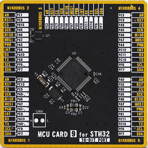
Type
8th Generation
Architecture
ARM Cortex-M4
MCU Memory (KB)
256
Silicon Vendor
STMicroelectronics
Pin count
64
RAM (Bytes)
32768
Used MCU Pins
mikroBUS™ mapper
Take a closer look
Click board™ Schematic
Step by step
Project assembly

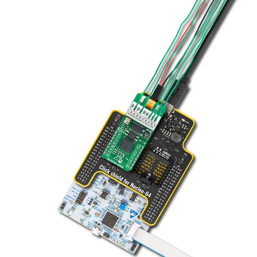
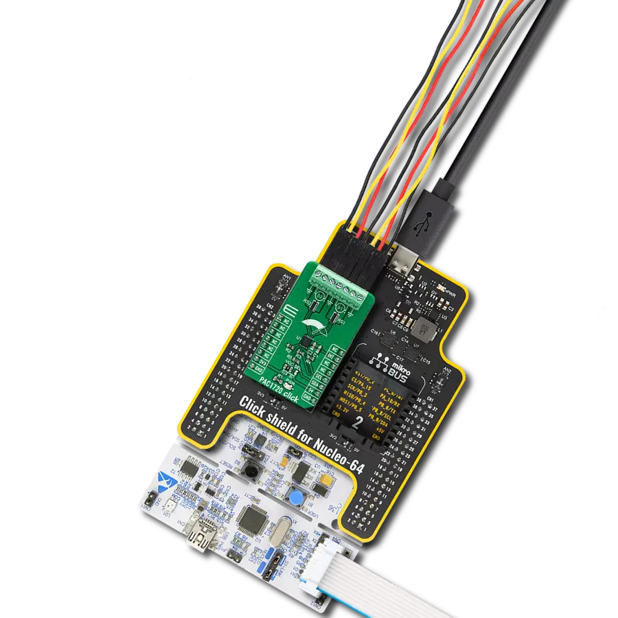
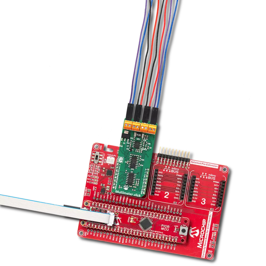
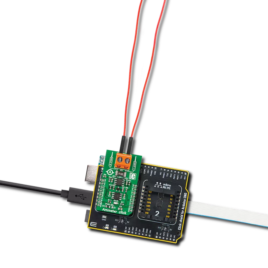
Start by selecting your development board and Click board™. Begin with the Fusion for STM32 v8 as your development board.


Software Support
Library Description
This library contains API for Hz To V 2 Click driver.
Key functions:
hztov2_en_pin- This function enable the click boardhztov2_read_voltage- This function read ADC data and converts it to voltagehztov2_fin_set- This function sets PWM clock frequency at FIN pin.
Open Source
Code example
The complete application code and a ready-to-use project are available through the NECTO Studio Package Manager for direct installation in the NECTO Studio. The application code can also be found on the MIKROE GitHub account.
/*!
 * \file
 * \brief HzToV2 Click example
 *
 * # Description
 * This app converts input frequency to a DC voltage output.
 *
 * The demo application is composed of two sections :
 *
 * ## Application Init
 * This function initializes and configures the logger and the Click board.
 *
 * ## Application Task
 * Sets the PWM frequency then reads the voltage from VO pin and logs all data on USB UART.
 *
 * ## NOTE
 * In order to set PWM frequency below 1 kHz, the user will probably need to lower the main MCU clock frequency.
 *
 * \author MikroE Team
 *
 */
// ------------------------------------------------------------------- INCLUDES

#include "board.h"
#include "log.h"
#include "hztov2.h"

// ------------------------------------------------------------------ VARIABLES

static hztov2_t hztov2;
static log_t logger;
static float voltage;
static uint32_t fin;

// ------------------------------------------------------ APPLICATION FUNCTIONS

void application_init ( void )
{
    log_cfg_t log_cfg;
    hztov2_cfg_t cfg;

    /**
     * Logger initialization.
     * Default baud rate: 115200
     * Default log level: LOG_LEVEL_DEBUG
     * @note If USB_UART_RX and USB_UART_TX
     * are defined as HAL_PIN_NC, you will
     * need to define them manually for log to work.
     * See @b LOG_MAP_USB_UART macro definition for detailed explanation.
     */
    LOG_MAP_USB_UART( log_cfg );
    log_init( &logger, &log_cfg );
    log_info( &logger, "---- Application Init ----" );

    //  Click initialization.

    hztov2_cfg_setup( &cfg );
    HZTOV2_MAP_MIKROBUS( cfg, MIKROBUS_1 );
    hztov2_init( &hztov2, &cfg );
    hztov2_en_pin( &hztov2, 1 );

    fin = 10000;

    Delay_ms ( 100 );
}

void application_task ( void )
{
    if ( fin > 120000 )
        fin = 10000;
    hztov2_fin_set( &hztov2, fin );
    log_printf( &logger, "Frequency: %lu Hz \r\n", fin );
    Delay_ms ( 100 );

    voltage = hztov2_read_voltage( &hztov2 );
    log_printf( &logger, "Voltage: %.2f V \r\n", voltage );

    fin += 10000;
    Delay_ms ( 1000 );
    Delay_ms ( 1000 );
}

int main ( void )
{
    /* Do not remove this line or clock might not be set correctly. */
    #ifdef PREINIT_SUPPORTED
    preinit();
    #endif

    application_init( );

    for ( ; ; )
    {
        application_task( );
    }

    return 0;
}

// ------------------------------------------------------------------------ END
Additional Support
Resources
Category:Measurements