Convert the countless reams of digital information into analog signals using DAC104S085 and PIC18F4685
From digits to signals
Published Aug 18, 2023
Click board™
DAC 6 Click
Dev. board
EasyPIC v7
Compiler
NECTO Studio
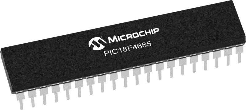
MCU
PIC18F4685
As digital information converges into analog clarity, our solution fosters connectivity by enabling effective communication between systems, unlocking a realm of data transformation possibilities
A
A
Hardware Overview
How does it work?
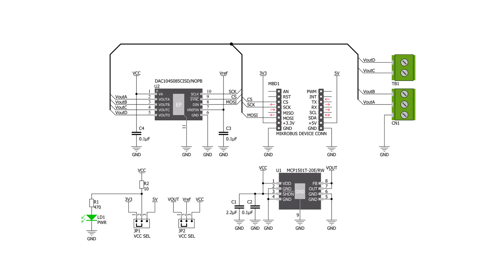
DAC 6 Click is based on the DAC104S085, 10-bit resolution micro-power QUAD digital-to-analog converter with rail-to-rail output from Texas Instruments. The DAC104S085 is manufactured on a CMOS process with an architecture consisting of switches and resistor strings followed by an output buffer. The reference voltage is applied at the VREFIN pin and is shared by all four DAC outputs (A, B, C, and D). This string consists of 1024 equal-valued resistors with a switch at each junction of two resistors, plus a switch to the ground. The code loaded into the DAC register determines which switch is closed, connecting the proper node to the amplifier. The voltage reference pin of the DAC104S085 is not buffered, and because of that, it is recommended to drive the VREFIN pin by a voltage source with a low output impedance.
This is accomplished using the MCP1501, a low drift bandgap-based voltage reference from a Microchip capable of sinking and sourcing 20mA of current. The bandgap uses chopper-based amplifiers, effectively reducing the drift to zero. The reference voltage range which can be applied to the VREFIN pin is 1V to VCC (in this case, 2.048V), providing the widest possible output dynamic range with a maximum output current of 11mA per channel. The DAC 6 Click communicates with MCU using the 3-Wire SPI serial interface compatible with standard SPI, QSPI™, and MICROWIRE™ and operates at clock rates up to 40 MHz. To use the full dynamic range of the DAC104S085, it is possible to connect the VREFIN pin to the supply voltage VCC. Because of its low power consumption, a reference source may be
used as the reference input or the supply voltage, which results in accuracy and stability. The reference voltage level can be selected by positioning the SMD jumper labeled as VREF SEL to an appropriate position, selecting between a value of 2.048V and the supply voltage VCC. This Click Board™ uses the SPI communication interface with both 3.3V and 5V. The onboard SMD jumper labeled VCC SEL allows voltage selection for interfacing with 3.3V and 5V MCUs. More information about the DAC104S085’s functionality, electrical specifications, and typical performance can be found in the attached datasheet. However, the Click board™ comes equipped with a library that contains easy-to-use functions and a usage example that may be used as a reference for the development.

Features overview
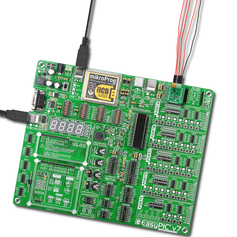
Development board
EasyPIC v7 is the seventh generation of PIC development boards specially designed to develop embedded applications rapidly. It supports a wide range of 8-bit PIC microcontrollers from Microchip and has a broad set of unique functions, such as a powerful onboard mikroProg programmer and In-Circuit debugger over USB-B. The development board is well organized and designed so that the end-user has all the necessary elements in one place, such as switches, buttons, indicators, connectors, and others. With four different connectors for each port, EasyPIC v7 allows you to connect accessory boards, sensors, and custom electronics more efficiently than ever. Each part of
the EasyPIC v7 development board contains the components necessary for the most efficient operation of the same board. An integrated mikroProg, a fast USB 2.0 programmer with mikroICD hardware In-Circuit Debugger, offers many valuable programming/debugging options and seamless integration with the Mikroe software environment. Besides it also includes a clean and regulated power supply block for the development board. It can use various external power sources, including an external 12V power supply, 7-23V AC or 9-32V DC via DC connector/screw terminals, and a power source via the USB Type-B (USB-B) connector. Communication options such as
USB-UART and RS-232 are also included, alongside the well-established mikroBUS™ standard, three display options (7-segment, graphical, and character-based LCD), and several different DIP sockets. These sockets cover a wide range of 8-bit PIC MCUs, from PIC10F, PIC12F, PIC16F, PIC16Enh, PIC18F, PIC18FJ, and PIC18FK families. EasyPIC v7 is an integral part of the Mikroe ecosystem for rapid development. Natively supported by Mikroe software tools, it covers many aspects of prototyping and development thanks to a considerable number of different Click boards™ (over a thousand boards), the number of which is growing every day.

Microcontroller Overview
MCU Card / MCU
Architecture
PIC
MCU Memory (KB)
96
Silicon Vendor
Microchip
Pin count
40
RAM (Bytes)
3328
Used MCU Pins
mikroBUS™ mapper
Take a closer look
Click board™ Schematic
Step by step
Project assembly

Start by selecting your development board and Click board™. Begin with the EasyPIC v7 as your development board.


Track your results in real time
Application Output
1. Application Output - In Debug mode, the 'Application Output' window enables real-time data monitoring, offering direct insight into execution results. Ensure proper data display by configuring the environment correctly using the provided tutorial.

2. UART Terminal - Use the UART Terminal to monitor data transmission via a USB to UART converter, allowing direct communication between the Click board™ and your development system. Configure the baud rate and other serial settings according to your project's requirements to ensure proper functionality. For step-by-step setup instructions, refer to the provided tutorial.

3. Plot Output - The Plot feature offers a powerful way to visualize real-time sensor data, enabling trend analysis, debugging, and comparison of multiple data points. To set it up correctly, follow the provided tutorial, which includes a step-by-step example of using the Plot feature to display Click board™ readings. To use the Plot feature in your code, use the function: plot(*insert_graph_name*, variable_name);. This is a general format, and it is up to the user to replace 'insert_graph_name' with the actual graph name and 'variable_name' with the parameter to be displayed.

Software Support
Library Description
This library contains API for DAC 6 Click driver.
Key functions:
dac6_set_output- Function is used to set operation mode output channel and leveldac6_write_data- Sends 16-bit data to the device's input shift register.
Open Source
Code example
The complete application code and a ready-to-use project are available through the NECTO Studio Package Manager for direct installation in the NECTO Studio. The application code can also be found on the MIKROE GitHub account.
/*!
 * \file
 * \brief Dac6 Click example
 *
 * # Description
 * DAC 6 Click carries 12-bit buffered Digital-to-Analog Converter. It converts digital value
 * to the corresponding voltage level using external voltage reference.
 *
 * The demo application is composed of two sections :
 *
 * ## Application Init
 * Initalizes SPI driver.
 *
 * ## Application Task
 * This example shows capabilities of DAC 6 Click by changeing
 * output values from 0 to the maximum output range on all four channels.
 * Output voltage is calculated by using the equation :
 * Vout = Vrefin * (set_out / 4095).
 *
 *
 * \author MikroE Team
 *
 */
// ------------------------------------------------------------------- INCLUDES

#include "board.h"
#include "log.h"
#include "dac6.h"

// ------------------------------------------------------------------ VARIABLES

static dac6_t dac6;
static log_t logger;

static uint16_t n_cnt;
static float v_out;

// ------------------------------------------------------ APPLICATION FUNCTIONS

void application_init ( void )
{
    log_cfg_t log_cfg;
    dac6_cfg_t cfg;

    /**
     * Logger initialization.
     * Default baud rate: 115200
     * Default log level: LOG_LEVEL_DEBUG
     * @note If USB_UART_RX and USB_UART_TX
     * are defined as HAL_PIN_NC, you will
     * need to define them manually for log to work.
     * See @b LOG_MAP_USB_UART macro definition for detailed explanation.
     */
    LOG_MAP_USB_UART( log_cfg );
    log_init( &logger, &log_cfg );
    log_info( &logger, "---- Application Init ----" );
    //  Click initialization.

    dac6_cfg_setup( &cfg );
    DAC6_MAP_MIKROBUS( cfg, MIKROBUS_1 );
    dac6_init( &dac6, &cfg );
}

void application_task ( void )
{
    for ( n_cnt = 0; n_cnt < 4096; n_cnt += 315 )
    {
        dac6.chan    = DAC6_CHANNEL_A;
        dac6.op_mod  = DAC6_WRITE_SPEC_UPDATE_OUTPUT;
        dac6.v_ref   = DAC6_V_REF_2048;
        dac6.set_out = n_cnt;

        v_out = dac6_set_output( &dac6 );

        log_printf( &logger, " Channel  A : VOUT ~ %.2f mV\r\n", v_out );
        log_printf( &logger, "--------------------\r\n" );
        Delay_ms ( 1000 );
        Delay_ms ( 1000 );
        Delay_ms ( 1000 );
        Delay_ms ( 1000 );
        Delay_ms ( 1000 );
    }

    for ( n_cnt = 0; n_cnt < 4096; n_cnt += 315 )
    {
        dac6.chan    = DAC6_CHANNEL_B;
        dac6.op_mod  = DAC6_WRITE_SPEC_UPDATE_OUTPUT;
        dac6.v_ref   = DAC6_V_REF_2048;
        dac6.set_out = n_cnt;

        v_out = dac6_set_output( &dac6 );

        log_printf( &logger, " Channel  B : VOUT ~ %.2f mV\r\n", v_out );
        log_printf( &logger, "--------------------\r\n" );
        Delay_ms ( 1000 );
        Delay_ms ( 1000 );
        Delay_ms ( 1000 );
        Delay_ms ( 1000 );
        Delay_ms ( 1000 );
    }

    for ( n_cnt = 0; n_cnt < 4096; n_cnt += 315 )
    {
        dac6.chan    = DAC6_CHANNEL_C;
        dac6.op_mod  = DAC6_WRITE_SPEC_UPDATE_OUTPUT;
        dac6.v_ref   = DAC6_V_REF_2048;
        dac6.set_out = n_cnt;

        v_out = dac6_set_output( &dac6 );

        log_printf( &logger, " Channel  C : VOUT ~ %.2f mV\r\n", v_out );
        log_printf( &logger, "--------------------\r\n" );
        Delay_ms ( 1000 );
        Delay_ms ( 1000 );
        Delay_ms ( 1000 );
        Delay_ms ( 1000 );
        Delay_ms ( 1000 );
    }

    for ( n_cnt = 0; n_cnt < 4096; n_cnt += 315 )
    {
        dac6.chan    = DAC6_CHANNEL_D;
        dac6.op_mod  = DAC6_WRITE_SPEC_UPDATE_OUTPUT;
        dac6.v_ref   = DAC6_V_REF_2048;
        dac6.set_out = n_cnt;

        v_out = dac6_set_output( &dac6 );

        log_printf( &logger, " Channel  D : VOUT ~ %.2f mV\r\n", v_out );
        log_printf( &logger, "--------------------\r\n" );
        Delay_ms ( 1000 );
        Delay_ms ( 1000 );
        Delay_ms ( 1000 );
        Delay_ms ( 1000 );
        Delay_ms ( 1000 );
    }

    Delay_ms ( 1000 );
}

int main ( void )
{
    /* Do not remove this line or clock might not be set correctly. */
    #ifdef PREINIT_SUPPORTED
    preinit();
    #endif

    application_init( );

    for ( ; ; )
    {
        application_task( );
    }

    return 0;
}


// ------------------------------------------------------------------------ END