Convert analog voltage into PWM signals with LTC6992CS6-1 and MK22FN512VLH12
Generate PWM signals at frequencies up to 1 MHz, providing flexibility for high-speed applications

Published Mar 15, 2024
Click board™
AN to PWM 2 Click
Dev. board
Kinetis Clicker
Compiler
NECTO Studio
MCU
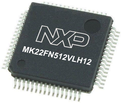
MK22FN512VLH12
Achieve precise analog-to-PWM signal conversion, enabling smooth control over devices like LEDs, heaters, and servo motors with minimal effort
A
A
Hardware Overview
How does it work?
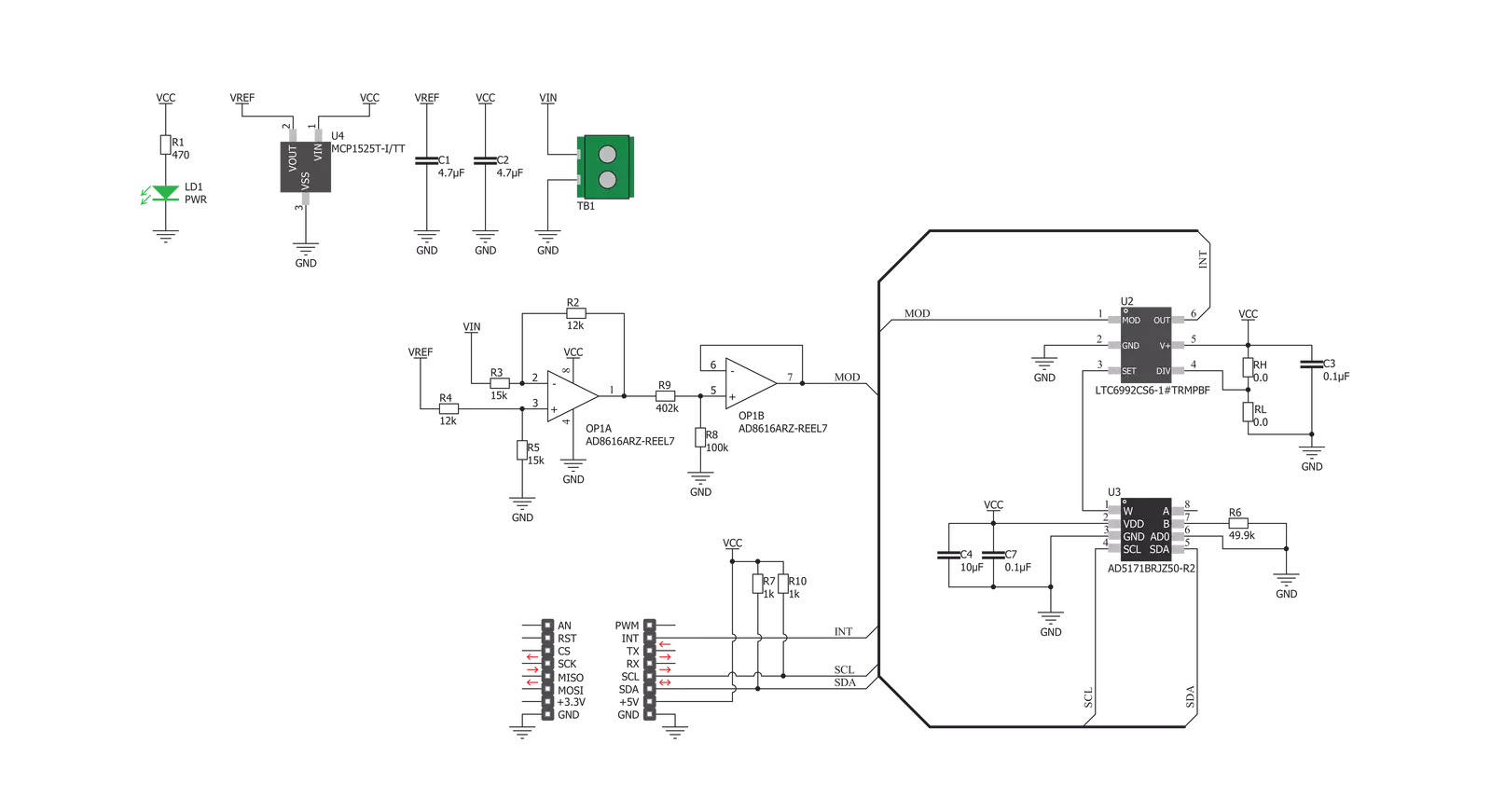
AN to PWM 2 Click is based on the LTC6992CS6, a voltage-controlled PWM generator from Analog Devices. This device is chosen because it keeps its output clocking at all times and offers glitch-free, a first cycle-accurate startup within 500μs of Power-On. The output of this Click board™ can source or sink up to 16 mA, and it has a linear response, so applying a voltage in a range of -2.5 to 2.5V on its input will result in generating the PWM pulse train with a duty cycle linearly proportional to the input voltage. The output PWM signal is brought to the INT pin of the mikroBUS™ socket to enable fast and precise duty cycle measurement using the interrupt routines. The LTC6992CS6 has a MOD pin, which represents pulse-width modulation input where it is necessary to bring an analog signal. To bring the corresponding signal to that pin, this Click
board™ uses an analog circuitry made of OpAmp AD8616ARZ from Analog Devices. In the first part of the circuit, amplifier OPA1 adjusts the input signal through a reference voltage of 2.5V by the MCP1525 from Microchip and applies input voltage in a range of -2.5 to 2.5V. The next part of the circuit is the voltage divider and amplifier OPA2, which has the function of a buffer, after which the signal required by the MOD pin of the LTC6992CS6 is obtained. The output frequency can range up from 3.81Hz to 1MHz and is controlled via the AD5171, a 64-position (OTP) digital potentiometer from Analog Devices, which programs the LTC6992CS6’s internal master oscillator frequency. The output frequency is determined by this master oscillator and an internal frequency divider programmable to eight settings from 1 to 16384. It
communicates with MCU using the standard I2C serial interface that operates at clock rates up to 400 kHz and represents the most accurate way to set the frequency. It also left the possibility of adjusting the frequency via resistors RH and RL by placing appropriate resistors. This Click board™ is designed to be operated only with a 5V logic level. A proper logic voltage level conversion should be performed before the AN to PWM 2 Click is used with MCUs with different logic levels. More information about the LTC6992CS6’s functionality, electrical specifications, and typical performance can be found in the attached datasheet. However, the Click board™ comes equipped with a library that contains easy-to-use functions and a usage example that can be used as a reference for the development.

Features overview
Development board
Kinetis Clicker is a compact starter development board that brings the flexibility of add-on Click boards™ to your favorite microcontroller, making it a perfect starter kit for implementing your ideas. It comes with an onboard 32-bit ARM Cortex-M4 microcontroller, the MK22FN512VLH12 from NXP Semiconductor, a USB connector, LED indicators, buttons, a mikroProg connector, and a header for interfacing with external electronics. Thanks to its compact design with clear and easy-recognizable silkscreen markings, it provides a fluid and immersive working experience, allowing access
anywhere and under any circumstances. Each part of the Kinetis Clicker development kit contains the components necessary for the most efficient operation of the same board. In addition to the possibility of choosing the Kinetis Clicker programming method, using USB HID mikroBootloader, or through an external mikroProg connector for Kinetis programmer, the Clicker board also includes a clean and regulated power supply module for the development kit. The USB-MiniAB connection provides up to 500mA of current, which is more than enough to operate all
onboard and additional modules. All communication methods that mikroBUS™ itself supports are on this board, including the well-established mikroBUS™ socket, reset button, and several buttons and LED indicators. Kinetis Clicker is an integral part of the Mikroe ecosystem, allowing you to create a new application in minutes. Natively supported by Mikroe software tools, it covers many aspects of prototyping thanks to a considerable number of different Click boards™ (over a thousand boards), the number of which is growing every day.

Microcontroller Overview
MCU Card / MCU
Architecture
ARM Cortex-M4
MCU Memory (KB)
512
Silicon Vendor
NXP
Pin count
64
RAM (Bytes)
131072
Used MCU Pins
mikroBUS™ mapper
Take a closer look
Click board™ Schematic
Step by step
Project assembly

Start by selecting your development board and Click board™. Begin with the Kinetis Clicker as your development board.


Software Support
Library Description
This library contains API for AN to PWM 2 Click driver.
Key functions:
antopwm2_set_frequency- This function sets a frequency output in a range from 500kHz to 1MHz by setting the digipot resistanceantopwm2_set_frequency_otp- This function sets a frequency output in a range from 500kHz to 1MHz by setting the digipot resistance in OTP mode
Open Source
Code example
The complete application code and a ready-to-use project are available through the NECTO Studio Package Manager for direct installation in the NECTO Studio. The application code can also be found on the MIKROE GitHub account.
/*!
 * @file main.c
 * @brief AN to PWM 2 Click example
 *
 * # Description
 * This example demonstrates the use of AN to PWM 2 Click board by changing the PWM output
 * frequency from 500kHz to 1MHz in steps of 50kHz.
 *
 * The demo application is composed of two sections :
 *
 * ## Application Init
 * Initializes the driver and logger.
 *
 * ## Application Task
 * Changes the PWM output frequency every 5 seconds in steps of 50kHz going through the full range
 * from 500kHz to 1MHz. The currently set frequency will be displayed on the USB UART.
 *
 * @note
 * Applying a voltage of -2.5 to 2.5V on the input will generate the PWM pulse train
 * with a duty cycle linearly proportional to the input voltage.
 *
 * @author Stefan Filipovic
 *
 */

#include "board.h"
#include "log.h"
#include "antopwm2.h"

static antopwm2_t antopwm2;
static log_t logger;

void application_init ( void )
{
    log_cfg_t log_cfg;  /**< Logger config object. */
    antopwm2_cfg_t antopwm2_cfg;  /**< Click config object. */

    /**
     * Logger initialization.
     * Default baud rate: 115200
     * Default log level: LOG_LEVEL_DEBUG
     * @note If USB_UART_RX and USB_UART_TX
     * are defined as HAL_PIN_NC, you will
     * need to define them manually for log to work.
     * See @b LOG_MAP_USB_UART macro definition for detailed explanation.
     */
    LOG_MAP_USB_UART( log_cfg );
    log_init( &logger, &log_cfg );
    log_info( &logger, " Application Init " );

    // Click initialization.
    antopwm2_cfg_setup( &antopwm2_cfg );
    ANTOPWM2_MAP_MIKROBUS( antopwm2_cfg, MIKROBUS_1 );
    if ( I2C_MASTER_ERROR == antopwm2_init( &antopwm2, &antopwm2_cfg ) )
    {
        log_error( &logger, " Communication init." );
        for ( ; ; );
    }

    log_info( &logger, " Application Task " );
}

void application_task ( void )
{
    static uint32_t freq = ANTOPWM2_FREQ_MIN;
    if ( ANTOPWM2_OK == antopwm2_set_frequency ( &antopwm2, freq ) )
    {
        log_printf ( &logger, " Frequency: %lu Hz\r\n\n", freq );
    }
    freq += 50000;
    if ( freq > ANTOPWM2_FREQ_MAX )
    {
        freq = ANTOPWM2_FREQ_MIN;
    }
    Delay_ms ( 1000 );
    Delay_ms ( 1000 );
    Delay_ms ( 1000 );
    Delay_ms ( 1000 );
    Delay_ms ( 1000 );
}

int main ( void )
{
    /* Do not remove this line or clock might not be set correctly. */
    #ifdef PREINIT_SUPPORTED
    preinit();
    #endif

    application_init( );

    for ( ; ; )
    {
        application_task( );
    }

    return 0;
}

// ------------------------------------------------------------------------ END
Additional Support
Resources
Category:ADC


