Efficiently reduce higher voltages to lower values with MCP16331 and MK64FN1M0VDC12
Small size, big power

Published Jul 30, 2023
Click board™
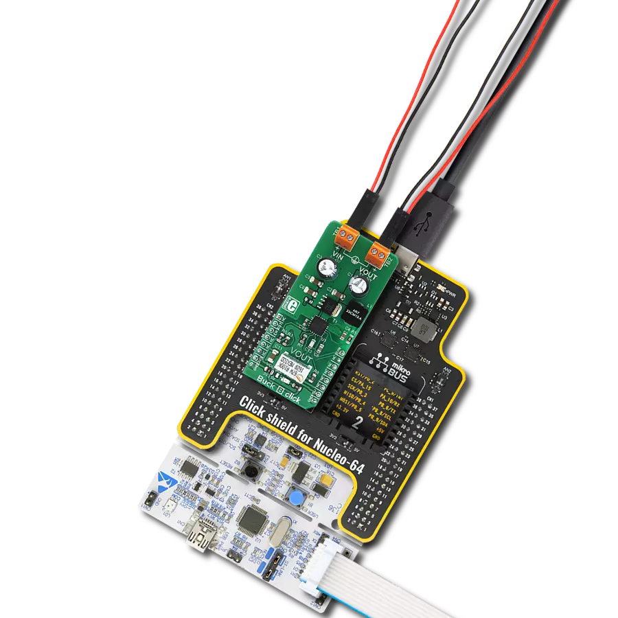
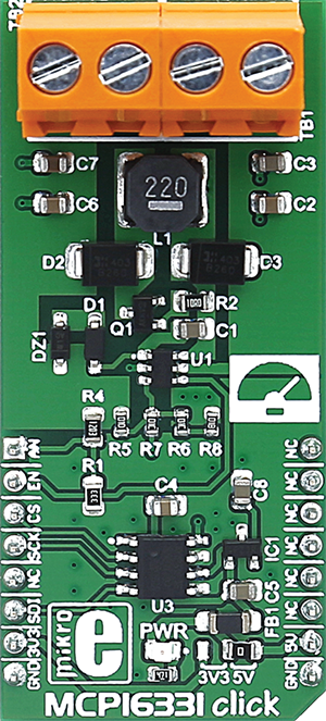
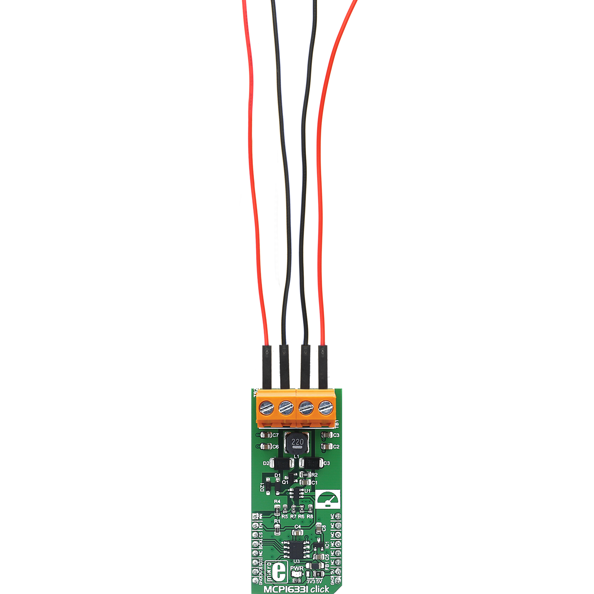
MCP16331 Click
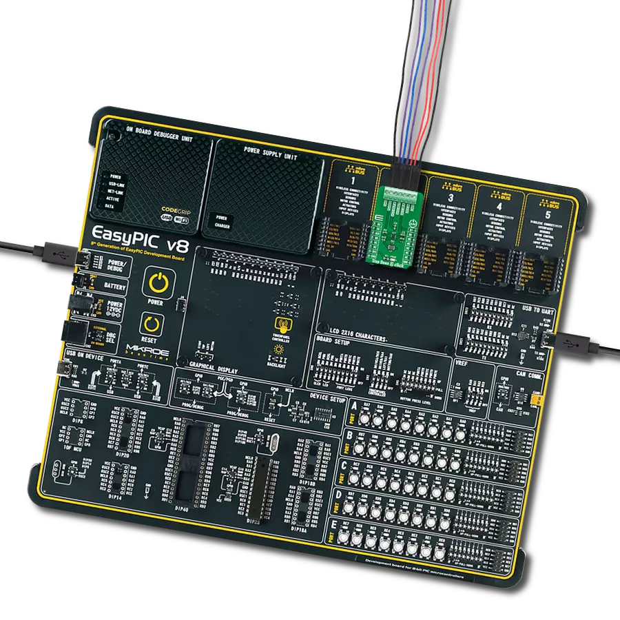
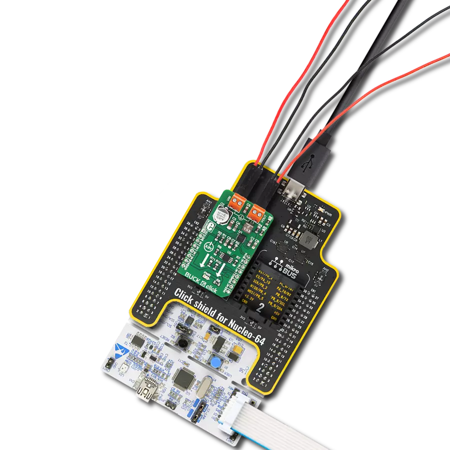
Dev. board
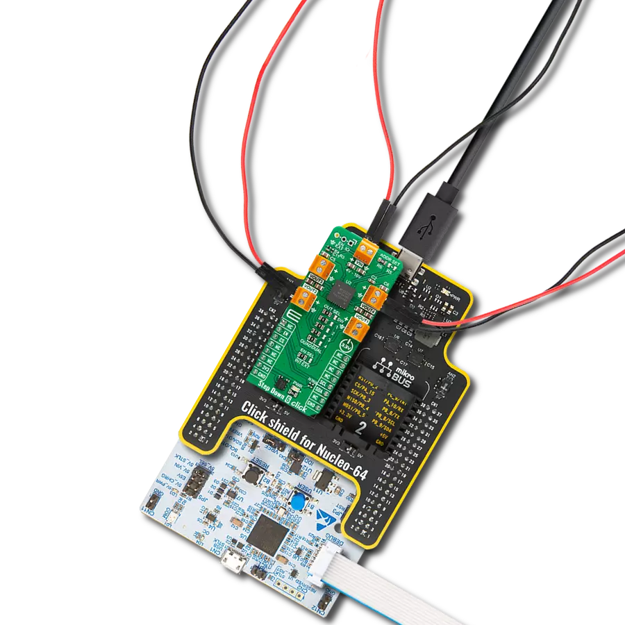
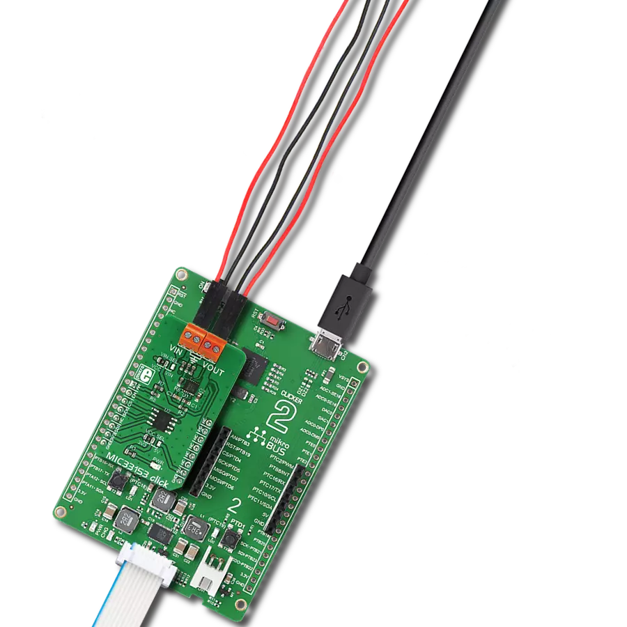
Clicker 2 for Kinetis
Compiler
NECTO Studio
MCU
MK64FN1M0VDC12
This high-efficiency buck regulator stands as a beacon of power management, delivering superior voltage conversion while minimizing energy losses
A
A
Hardware Overview
How does it work?
MCP16331 Click is based on the MCP16331, a non-synchronous, step-down converter from Microchip capable of stepping input voltages ranging from 4.4V to 50V and output voltage ranging from 2.0V to 24V. More details about the MCP16331 are available in the official datasheet. However, the MCP16331 click is designed to handle an input voltage ranging from 4.5V to 18V and output a voltage ranging from 2,25V to 12V at 500 mA maximum current since it works in a buck-boost topology. To set the output voltage of the MCP16331 click, the MCP4921 - a low-power 12-Bit dual voltage output DAC is used in the feedback loop. The output of this DAC is used to drive the FB pin of the MCP16331, so to set up the output voltage, it is enough to set the DAC output to a specific value. This will cause the FB pin to drive
the switching section of the MCP16331, which will output a desired voltage level as a result. The AN pin of the mikroBUS™ can be used to verify the output voltage and correct the value given to the DAC if needed. The MCP4291 DAC can be configured by the host MCU via the SPI bus pins, routed to the mikroBUS™. The AN pin of the mikroBUS™ is routed to a middle point of a voltage divider on the output. This voltage divider is used to scale down the output voltage so the ADC of the host MCU can successfully convert it. Besides the bit depth of the ADC, this should also be considered when calculating the output voltage value. The MCP16331 click has two screw terminals used to connect the input voltage and the load, and the SMD jumper is used to select the voltage for the DAC IC. This affects the SPI logic
voltage levels, so both 3.3V and 5V MCUs can be used with this Click board™. This sequence is because the enable pin (EN) of the MCP16331 has an internal pull-up resistor that keeps the MCP16331 output stage enabled even if the pin is left unconnected. At power-up, before you set the voltage via SPI, DAC output is unspecified, and the output voltage may be set higher than what your load supports. This Click board™ can operate with either 3.3V or 5V logic voltage levels selected via an onboard jumper. This way, both 3.3V and 5V capable MCUs can use the communication lines properly. Also, this Click board™ comes equipped with a library containing easy-to-use functions and an example code that can be used, as a reference, for further development.

Features overview
Development board
Clicker 2 for Kinetis is a compact starter development board that brings the flexibility of add-on Click boards™ to your favorite microcontroller, making it a perfect starter kit for implementing your ideas. It comes with an onboard 32-bit ARM Cortex-M4F microcontroller, the MK64FN1M0VDC12 from NXP Semiconductors, two mikroBUS™ sockets for Click board™ connectivity, a USB connector, LED indicators, buttons, a JTAG programmer connector, and two 26-pin headers for interfacing with external electronics. Its compact design with clear and easily recognizable silkscreen markings allows you to build gadgets with unique functionalities and
features quickly. Each part of the Clicker 2 for Kinetis development kit contains the components necessary for the most efficient operation of the same board. In addition to the possibility of choosing the Clicker 2 for Kinetis programming method, using a USB HID mikroBootloader or an external mikroProg connector for Kinetis programmer, the Clicker 2 board also includes a clean and regulated power supply module for the development kit. It provides two ways of board-powering; through the USB Micro-B cable, where onboard voltage regulators provide the appropriate voltage levels to each component on the board, or
using a Li-Polymer battery via an onboard battery connector. All communication methods that mikroBUS™ itself supports are on this board, including the well-established mikroBUS™ socket, reset button, and several user-configurable buttons and LED indicators. Clicker 2 for Kinetis is an integral part of the Mikroe ecosystem, allowing you to create a new application in minutes. Natively supported by Mikroe software tools, it covers many aspects of prototyping thanks to a considerable number of different Click boards™ (over a thousand boards), the number of which is growing every day.

Microcontroller Overview
MCU Card / MCU

Architecture
ARM Cortex-M4
MCU Memory (KB)
1024
Silicon Vendor
NXP
Pin count
121
RAM (Bytes)
262144
Used MCU Pins
mikroBUS™ mapper
Take a closer look
Click board™ Schematic

Step by step
Project assembly

Start by selecting your development board and Click board™. Begin with the Clicker 2 for Kinetis as your development board.


Track your results in real time
Application Output
1. Application Output - In Debug mode, the 'Application Output' window enables real-time data monitoring, offering direct insight into execution results. Ensure proper data display by configuring the environment correctly using the provided tutorial.

2. UART Terminal - Use the UART Terminal to monitor data transmission via a USB to UART converter, allowing direct communication between the Click board™ and your development system. Configure the baud rate and other serial settings according to your project's requirements to ensure proper functionality. For step-by-step setup instructions, refer to the provided tutorial.

3. Plot Output - The Plot feature offers a powerful way to visualize real-time sensor data, enabling trend analysis, debugging, and comparison of multiple data points. To set it up correctly, follow the provided tutorial, which includes a step-by-step example of using the Plot feature to display Click board™ readings. To use the Plot feature in your code, use the function: plot(*insert_graph_name*, variable_name);. This is a general format, and it is up to the user to replace 'insert_graph_name' with the actual graph name and 'variable_name' with the parameter to be displayed.

Software Support
Library Description
This library contains API for MCP16331 Click driver.
Key functions:
mcp16331_set_vout- This function sets the output voltage value
Open Source
Code example
The complete application code and a ready-to-use project are available through the NECTO Studio Package Manager for direct installation in the NECTO Studio. The application code can also be found on the MIKROE GitHub account.
/*!
 * \file
 * \brief Mcp16331 Click example
 *
 * # Description
 * This application is buck-boost voltage regulator.
 *
 * The demo application is composed of two sections :
 *
 * ## Application Init
 * Sends hal pointers, and initializes Click
 *
 * ## Application Task
 * Switches between 5 V and 12 V values
 *
 * \author MikroE Team
 *
 */
// ------------------------------------------------------------------- INCLUDES

#include "board.h"
#include "log.h"
#include "mcp16331.h"

// ------------------------------------------------------------------ VARIABLES

static mcp16331_t mcp16331;
static log_t logger;

// ------------------------------------------------------ APPLICATION FUNCTIONS

void application_init ( void )
{
    log_cfg_t log_cfg;
    mcp16331_cfg_t cfg;

    /**
     * Logger initialization.
     * Default baud rate: 115200
     * Default log level: LOG_LEVEL_DEBUG
     * @note If USB_UART_RX and USB_UART_TX
     * are defined as HAL_PIN_NC, you will
     * need to define them manually for log to work.
     * See @b LOG_MAP_USB_UART macro definition for detailed explanation.
     */
    LOG_MAP_USB_UART( log_cfg );
    log_init( &logger, &log_cfg );
    log_info( &logger, "---- Application Init ----" );

    //  Click initialization.

    mcp16331_cfg_setup( &cfg );
    MCP16331_MAP_MIKROBUS( cfg, MIKROBUS_1 );
    mcp16331_init( &mcp16331, &cfg );
}

void application_task ( void )
{
    mcp16331_set_vout( &mcp16331, 5000 );
    Delay_ms ( 1000 );
    Delay_ms ( 1000 );
    Delay_ms ( 1000 );
    mcp16331_set_vout( &mcp16331, 12000 );
    Delay_ms ( 1000 );
    Delay_ms ( 1000 );
    Delay_ms ( 1000 );
}

int main ( void )
{
    /* Do not remove this line or clock might not be set correctly. */
    #ifdef PREINIT_SUPPORTED
    preinit();
    #endif

    application_init( );

    for ( ; ; )
    {
        application_task( );
    }

    return 0;
}

// ------------------------------------------------------------------------ END