Transform device-to-cloud communication with NTP5332 and MK64FN1M0VDC12
NFC forum-compliant I2C bridge
Published May 31, 2023
Click board™
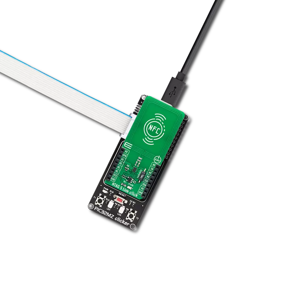
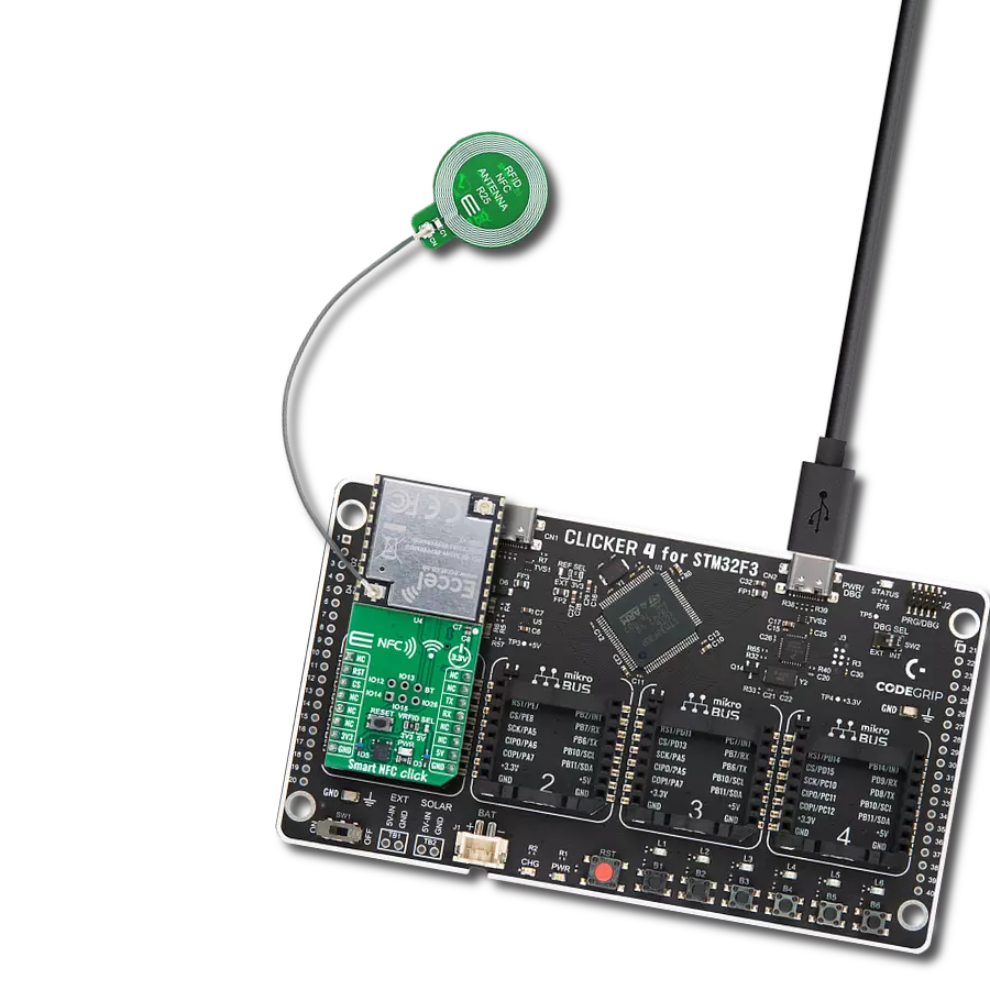
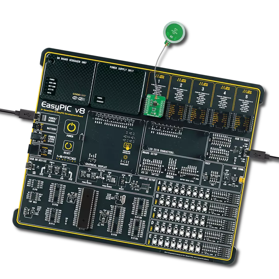
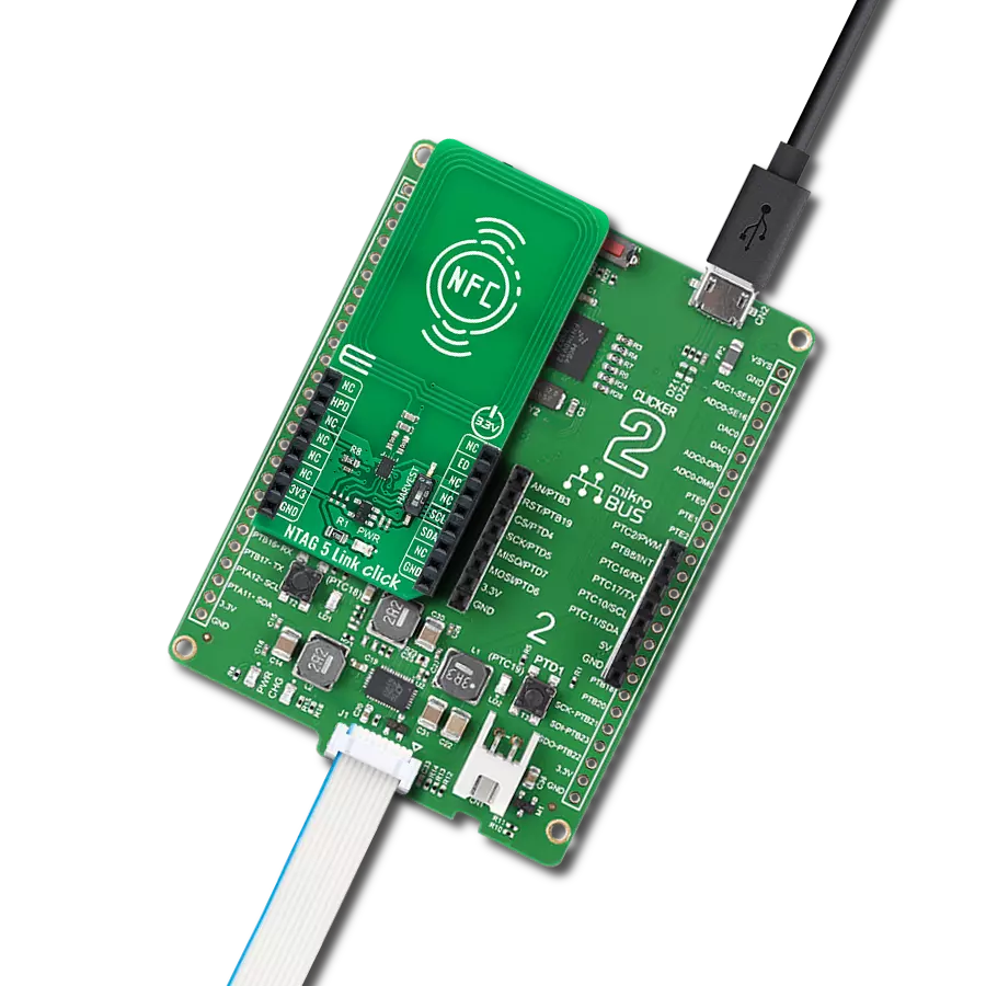
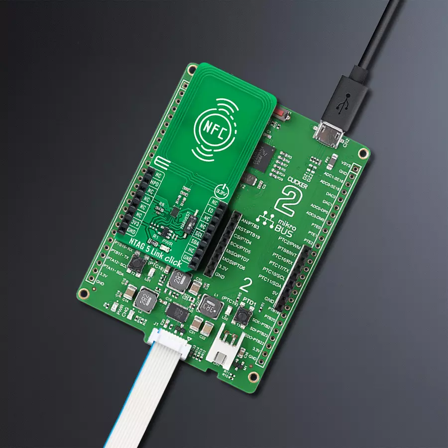
NTAG 5 Link Click
Dev. board
Clicker 2 for Kinetis
Compiler
NECTO Studio
MCU
MK64FN1M0VDC12
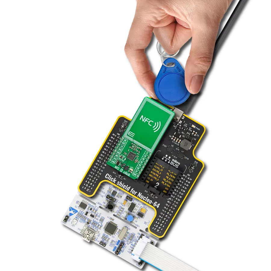
Experience the future-proof security with thishighly integrated NFC solution, forging a standard-based link from device to cloud
A
A
Hardware Overview
How does it work?
NTAG 5 Link Click is based on the NTP5332, a highly integrated NFC IC optimized for sensor-driven applications that act as a bridge between an NFC-enabled device and any I2C slave from NXP Semiconductors. This highly integrated NFC IC creates a secure, standard-based link from the device to the cloud in a future-proof way to address and even power sensors. Operating at 13.56 MHz, the NTP5332 is an NFC Forum Type 5 Tag, which can be read and written by an NFC-enabled device at close range and an ISO/IEC 15693-enabled industrial reader over a more extended range (>60cm). With NTAG 5 Link, the device can connect to the cloud with a single tap. The connection uses an NFC Forum-compliant data exchange mechanism involving SRAM to ensure interoperable data transfers. Also, it offers 2048 bytes of memory divided into three areas where each area can use a different protection level, varying from no protection to 32-/64-bit password-protected read/write access or up to 128-bit-AES mutual authentication protected read/write access. The NTAG 5 Link comes with pre-programmed proof-of-origin functionality to verify
authenticity. The ECC-based originality signature can be reprogrammed or locked by the customer through its registers. This Click board™ communicates with MCU using the standard I2C 2-Wire interface to read data and configure settings, supporting Standard Mode operation with a clock frequency of 100kHz and Fast Mode up to 400kHz. The NTP5332 also offers a transparent I2C master mode, for example, to read sensors without a microcontroller. The RF interface initiates an I2C Master communication, which can trigger a read or write transaction to an external I2C slave. Alongside this feature, an integrated SRAM is used as intermediate data storage. Session registers reflect the status of the I2C Master transaction. Therefore an RF reader has to poll for the status bits related to I2C Master to know the status of the current I2C transaction. The NTAG 5 Link can also operate as a standalone solution by drawing power from the NFC field of an NFC device. It supports an energy harvesting feature, activated by an onboard switch marked as HARVEST, which means it can supply power to other components in the system, in this case,
to supply the NTP5332. NTAG 5 Link can provide a fixed configurable voltage level of 1.8V, 2.4V, or 3V, selectable through register configuration when sufficient energy is available. In addition, this Click board™ can be placed in a hard power-down mode by setting the HPD pin routed on the RST pin of the mikroBUS™ socket. Besides, it also has an event detection and field detection functionality that defines the ED pin's behavior routed on the INT pin of the mikroBUS™ socket. This pin's behavior depends on various events such as the presence/absence of the NFC field, arbiter locked/unlocked EEPROM to NFC interface, Write/Read command ongoing, and more. This Click board™ can only be operated with a 3.3V logic voltage level. The board must perform appropriate logic voltage level conversion before using MCUs with different logic levels. However, the Click board™ comes equipped with a library containing functions and an example code that can be used as a reference for further development.


Features overview
Development board
Clicker 2 for Kinetis is a compact starter development board that brings the flexibility of add-on Click boards™ to your favorite microcontroller, making it a perfect starter kit for implementing your ideas. It comes with an onboard 32-bit ARM Cortex-M4F microcontroller, the MK64FN1M0VDC12 from NXP Semiconductors, two mikroBUS™ sockets for Click board™ connectivity, a USB connector, LED indicators, buttons, a JTAG programmer connector, and two 26-pin headers for interfacing with external electronics. Its compact design with clear and easily recognizable silkscreen markings allows you to build gadgets with unique functionalities and
features quickly. Each part of the Clicker 2 for Kinetis development kit contains the components necessary for the most efficient operation of the same board. In addition to the possibility of choosing the Clicker 2 for Kinetis programming method, using a USB HID mikroBootloader or an external mikroProg connector for Kinetis programmer, the Clicker 2 board also includes a clean and regulated power supply module for the development kit. It provides two ways of board-powering; through the USB Micro-B cable, where onboard voltage regulators provide the appropriate voltage levels to each component on the board, or
using a Li-Polymer battery via an onboard battery connector. All communication methods that mikroBUS™ itself supports are on this board, including the well-established mikroBUS™ socket, reset button, and several user-configurable buttons and LED indicators. Clicker 2 for Kinetis is an integral part of the Mikroe ecosystem, allowing you to create a new application in minutes. Natively supported by Mikroe software tools, it covers many aspects of prototyping thanks to a considerable number of different Click boards™ (over a thousand boards), the number of which is growing every day.

Microcontroller Overview
MCU Card / MCU

Architecture
ARM Cortex-M4
MCU Memory (KB)
1024
Silicon Vendor
NXP
Pin count
121
RAM (Bytes)
262144
Used MCU Pins
mikroBUS™ mapper
Take a closer look
Click board™ Schematic

Step by step
Project assembly

Start by selecting your development board and Click board™. Begin with the Clicker 2 for Kinetis as your development board.


Software Support
Library Description
This library contains API for NTAG 5 Link Click driver.
Key functions:
ntag5link_write_ndef_uri_recordThis function writes specific NDEF URI record to the memory address specified with NTAG5LINK_NDEF_MESSAGE_START_ADDRESS macro.ntag5link_write_message_to_memoryThis function writes a specified number of data bytes to the user memory starting from block_addr.ntag5link_read_message_from_memoryThis function reads a specified number of data bytes from the user memory starting from @b block_addr.
Open Source
Code example
The complete application code and a ready-to-use project are available through the NECTO Studio Package Manager for direct installation in the NECTO Studio. The application code can also be found on the MIKROE GitHub account.
/*!
 * @file main.c
 * @brief NTAG5Link Click example
 *
 * # Description
 * This example demonstrates the use of NTAG 5 Link Click board by programming the
 * specified NDEF URI record to the memory, and showing the memory read/write feature.
 *
 * The demo application is composed of two sections :
 *
 * ## Application Init
 * Initializes the driver and logger and performs the Click default configuration which
 * enables the device and formats its user memory. After that it programs the specified
 * NDEF URI record to the memory.
 *
 * ## Application Task
 * Writes a desired number of data bytes to the memory and verifies that it is written
 * correctly by reading from the same memory location and displaying the memory content
 * on the USB UART approximately every 5 seconds.
 *
 * @author Stefan Filipovic
 *
 */

#include "board.h"
#include "log.h"
#include "ntag5link.h"

/**
 * URL to store to memory as NDEF URI record
 */
#define URI_DATA                "www.mikroe.com/ntag-5-link-click"

/**
 * Starting block address to where the text message will be stored
 * Must be > ( NTAG5LINK_NDEF_MESSAGE_START_ADDRESS + sizeof ( URI_DATA ) / NTAG5LINK_MEMORY_BLOCK_SIZE + 3 )
 * to avoid overwriting NDEF URI record.
 */
#define TEXT_MESSAGE_ADDRESS    0x0040

/**
 * Text message content that will be stored to memory
 */
#define TEXT_MESSAGE            "MikroE - NTAG 5 Link Click"

static ntag5link_t ntag5link;
static log_t logger;

void application_init ( void )
{
    log_cfg_t log_cfg;  /**< Logger config object. */
    ntag5link_cfg_t ntag5link_cfg;  /**< Click config object. */

    /**
     * Logger initialization.
     * Default baud rate: 115200
     * Default log level: LOG_LEVEL_DEBUG
     * @note If USB_UART_RX and USB_UART_TX
     * are defined as HAL_PIN_NC, you will
     * need to define them manually for log to work.
     * See @b LOG_MAP_USB_UART macro definition for detailed explanation.
     */
    LOG_MAP_USB_UART( log_cfg );
    log_init( &logger, &log_cfg );
    log_info( &logger, " Application Init " );

    // Click initialization.
    ntag5link_cfg_setup( &ntag5link_cfg );
    NTAG5LINK_MAP_MIKROBUS( ntag5link_cfg, MIKROBUS_1 );
    if ( I2C_MASTER_ERROR == ntag5link_init( &ntag5link, &ntag5link_cfg ) )
    {
        log_error( &logger, " Communication init." );
        for ( ; ; );
    }

    if ( NTAG5LINK_ERROR == ntag5link_default_cfg ( &ntag5link ) )
    {
        log_error( &logger, " Default configuration." );
        for ( ; ; );
    }

    if ( NTAG5LINK_OK == ntag5link_write_ndef_uri_record ( &ntag5link, NTAG5LINK_URI_PREFIX_4,
                                                           URI_DATA, strlen ( URI_DATA ) ) )
    {
        log_printf( &logger, " NDEF URI record \"https://%s\" has been written\r\n", ( char * ) URI_DATA );
    }

    log_info( &logger, " Application Task " );
}

void application_task ( void )
{
    uint8_t message_buf[ 100 ] = { 0 };
    if ( NTAG5LINK_OK == ntag5link_write_message_to_memory ( &ntag5link,
                                                             TEXT_MESSAGE_ADDRESS,
                                                             TEXT_MESSAGE,
                                                             strlen ( TEXT_MESSAGE ) ) )
    {
        log_printf( &logger, " \"%s\" has been written to memory address 0x%.4X \r\n",
                    ( char * ) TEXT_MESSAGE, ( uint16_t ) TEXT_MESSAGE_ADDRESS );
    }
    if ( NTAG5LINK_OK == ntag5link_read_message_from_memory ( &ntag5link,
                                                              TEXT_MESSAGE_ADDRESS,
                                                              message_buf,
                                                              strlen ( TEXT_MESSAGE ) ) )
    {
        log_printf( &logger, " \"%s\" has been read from memory address 0x%.4X \r\n\n",
                    message_buf, ( uint16_t ) TEXT_MESSAGE_ADDRESS );
    }
    Delay_ms ( 1000 );
    Delay_ms ( 1000 );
    Delay_ms ( 1000 );
    Delay_ms ( 1000 );
    Delay_ms ( 1000 );
}

int main ( void )
{
    /* Do not remove this line or clock might not be set correctly. */
    #ifdef PREINIT_SUPPORTED
    preinit();
    #endif

    application_init( );

    for ( ; ; )
    {
        application_task( );
    }

    return 0;
}

// ------------------------------------------------------------------------ END
Additional Support
Resources
Category:RFID/NFC