Build a various waveform signal generator with AD9837 and TM4C123GH6PZ
Waves of Fun

Published May 27, 2023
Click board™
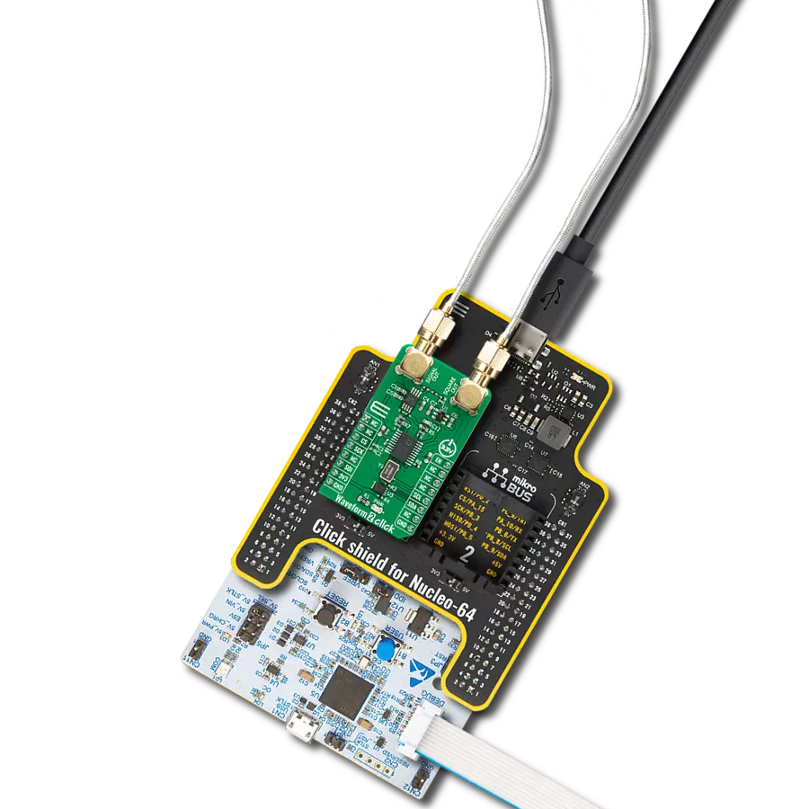
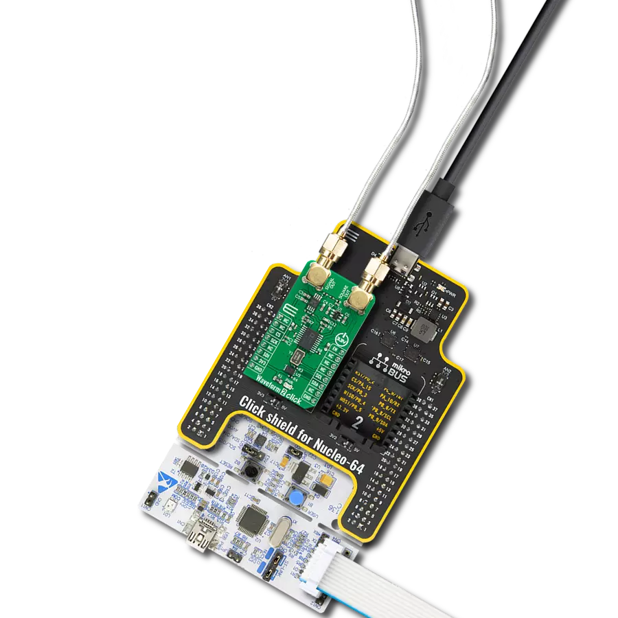
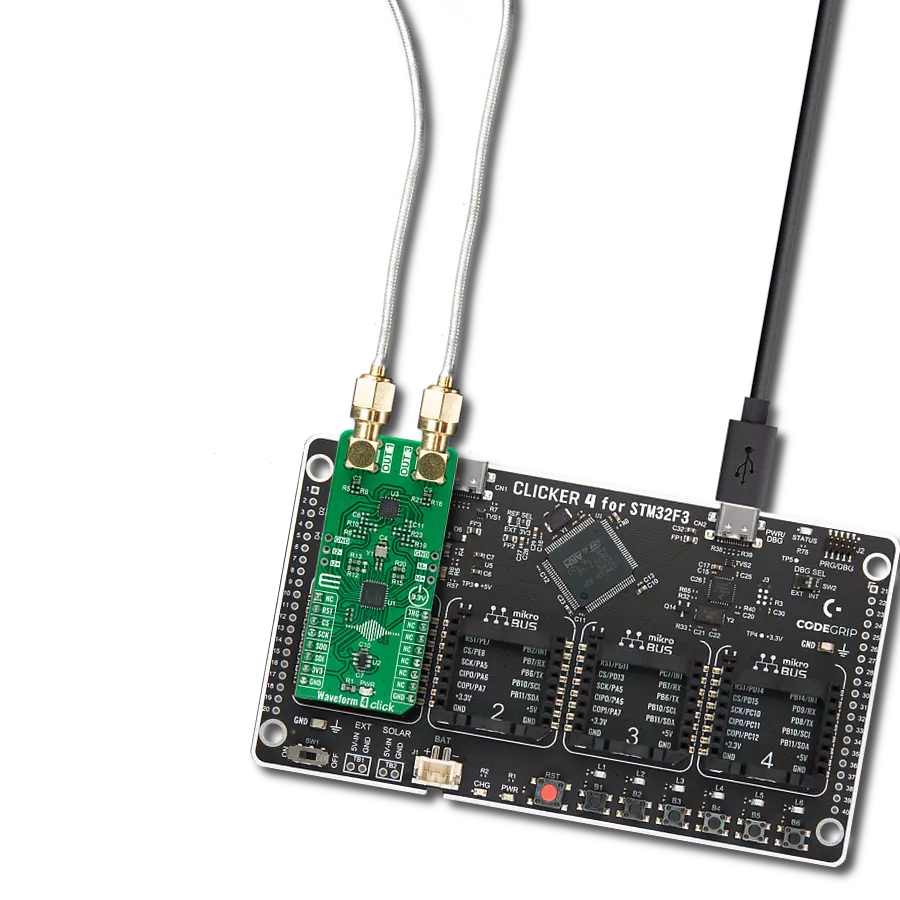
Waveform 3 Click
Dev. board
UNI Clicker
Compiler
NECTO Studio
MCU
TM4C123GH6PZ
Design and develop a waveform generator that produces specific waveforms to simulate sensor inputs for testing and validation purposes
A
A
Hardware Overview
How does it work?
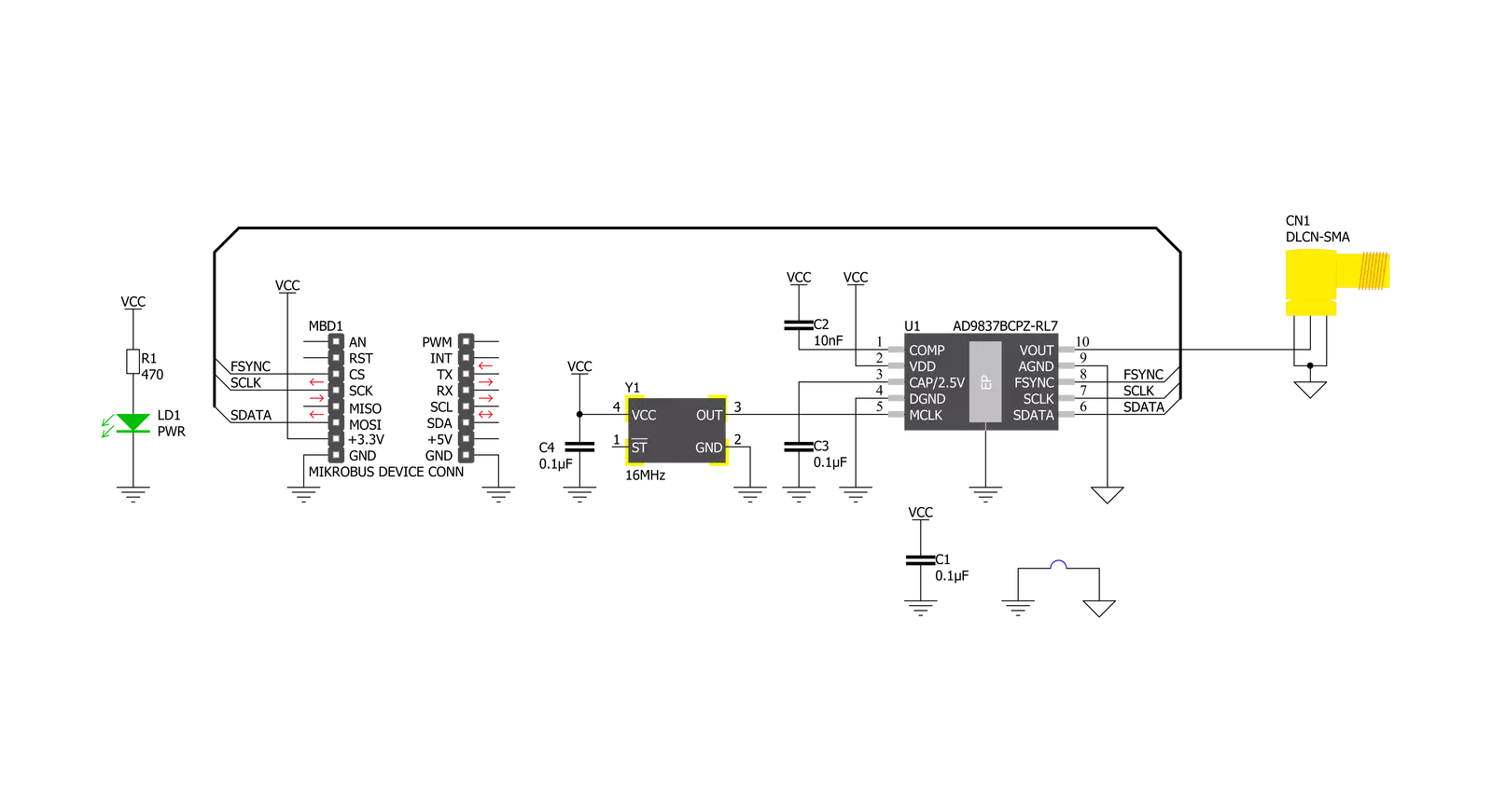
Waveform 3 Click is based on the AD9837, a fully integrated direct digital synthesis (DDS) device capable of producing high-performance sine and triangular wave outputs from Analog Devices. It also has an internal comparator that allows the creation of a square wave for clock generation. With 28-bit wide frequency registers, the output frequency and phase are software-programmable, allowing easy tuning. The AD9837 is capable of a broad range of complex and straightforward modulation schemes fully implemented in the digital domain, allowing the accurate and precise realization of complex modulation algorithms using DSP techniques. The internal circuitry of the AD9837 consists of a numerically controlled oscillator (NCO), frequency and phase modulators, SIN
ROM, a DAC, a comparator, and a regulator. Also, it has a high-performance, onboard 16MHz trimmed general oscillator that can serve as the master clock for the AD9837 achieving a resolution of 0.06Hz. The AD9837 offers a variety of outputs available from an onboard output SMA connector. The various output options (sine, triangular, and square wave) from the AD9837 make this Click board™ suitable for various applications, including modulation applications. It is also ideal for signal generator applications, and with its low current consumption, it is also suitable for applications in which it can serve as a local oscillator. The Waveform 3 Click communicates with MCU using the 3-Wire SPI serial interface compatible with standard SPI, QSPI™, MICROWIRE™, and DSP interface
standards and operates at clock rates up to 40MHz. Besides, it possesses additional functionality, such as a programmable Sleep function that allows external control of the Power-Down mode and Reset function, which resets the appropriate internal registers to 0 to provide an analog output of mid-scale. Remembering that the reset function does not reset the phase, frequency, or control registers is essential. This Click board™ can only be operated with a 3.3V logic voltage level. The board must perform appropriate logic voltage level conversion before using MCUs with different logic levels. However, the Click board™ comes equipped with a library containing functions and an example code that can be used as a reference for further development.


Features overview
Development board
UNI Clicker is a compact development board designed as a complete solution that brings the flexibility of add-on Click boards™ to your favorite microcontroller, making it a perfect starter kit for implementing your ideas. It supports a wide range of microcontrollers, such as different ARM, PIC32, dsPIC, PIC, and AVR from various vendors like Microchip, ST, NXP, and TI (regardless of their number of pins), four mikroBUS™ sockets for Click board™ connectivity, a USB connector, LED indicators, buttons, a debugger/programmer connector, and two 26-pin headers for interfacing with external electronics. Thanks to innovative manufacturing technology, it allows you to build
gadgets with unique functionalities and features quickly. Each part of the UNI Clicker development kit contains the components necessary for the most efficient operation of the same board. In addition to the possibility of choosing the UNI Clicker programming method, using a third-party programmer or CODEGRIP/mikroProg connected to onboard JTAG/SWD header, the UNI Clicker board also includes a clean and regulated power supply module for the development kit. It provides two ways of board-powering; through the USB Type-C (USB-C) connector, where onboard voltage regulators provide the appropriate voltage levels to each component on the board, or using a Li-Po/Li
Ion battery via an onboard battery connector. All communication methods that mikroBUS™ itself supports are on this board (plus USB HOST/DEVICE), including the well-established mikroBUS™ socket, a standardized socket for the MCU card (SiBRAIN standard), and several user-configurable buttons and LED indicators. UNI Clicker is an integral part of the Mikroe ecosystem, allowing you to create a new application in minutes. Natively supported by Mikroe software tools, it covers many aspects of prototyping thanks to a considerable number of different Click boards™ (over a thousand boards), the number of which is growing every day.

Microcontroller Overview
MCU Card / MCU
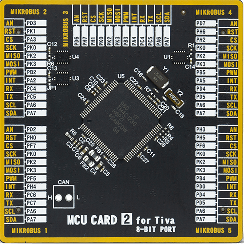
Type
8th Generation
Architecture
ARM Cortex-M4
MCU Memory (KB)
256
Silicon Vendor
Texas Instruments
Pin count
100
RAM (Bytes)
32768
Used MCU Pins
mikroBUS™ mapper
Take a closer look
Click board™ Schematic
Step by step
Project assembly

Start by selecting your development board and Click board™. Begin with the UNI Clicker as your development board.


Track your results in real time
Application Output
1. Application Output - In Debug mode, the 'Application Output' window enables real-time data monitoring, offering direct insight into execution results. Ensure proper data display by configuring the environment correctly using the provided tutorial.

2. UART Terminal - Use the UART Terminal to monitor data transmission via a USB to UART converter, allowing direct communication between the Click board™ and your development system. Configure the baud rate and other serial settings according to your project's requirements to ensure proper functionality. For step-by-step setup instructions, refer to the provided tutorial.

3. Plot Output - The Plot feature offers a powerful way to visualize real-time sensor data, enabling trend analysis, debugging, and comparison of multiple data points. To set it up correctly, follow the provided tutorial, which includes a step-by-step example of using the Plot feature to display Click board™ readings. To use the Plot feature in your code, use the function: plot(*insert_graph_name*, variable_name);. This is a general format, and it is up to the user to replace 'insert_graph_name' with the actual graph name and 'variable_name' with the parameter to be displayed.

Software Support
Library Description
This library contains API for Waveform 3 Click driver.
Key functions:
waveform3_cfg_setup- Config Object Initialization function.waveform3_init- Initialization function.waveform3_default_cfg- Click Default Configuration function.
Open Source
Code example
The complete application code and a ready-to-use project are available through the NECTO Studio Package Manager for direct installation in the NECTO Studio. The application code can also be found on the MIKROE GitHub account.
/*!
 * @file main.c
 * @brief Waveform3 Click example
 *
 * # Description
 * This demo app shows the basic capabilities of Waveform 3
 * Click board. First, the sinusoidal wave is incremented
 * to targeted frequency for visually pleasing introduction
 * after which it changes between 4 modes of output.
 *
 * The demo application is composed of two sections :
 *
 * ## Application Init
 * Application initializes the UART LOG and SPI drivers,
 * resets the device and sets frequency and phase shift to
 * default values. In the end, the mode is set with the
 * preferred freq and phase channel.
 *
 * ## Application Task
 * Task commences with the start frequency rising up to
 * the targeted one. When it reaches desired frequency,
 * the mode changes every 5 seconds which includes:
 * sinusoidal, triangular, DAC divided by 2 and DAC
 * outputs respectively.
 *
 * *note:*
 * Waveform 3 Click might not provide a high enough peak to peak signal on higher frequencies.
 * The user can freely implement custom buffer for the output stage.
 * Special thanks to my esteemed co-worker Nenad Filipovic for support during firmware development.
 *
 * @author Stefan Nikolic
 *
 */

#include "board.h"
#include "log.h"
#include "waveform3.h"

static waveform3_t waveform3;
static log_t logger;

static uint32_t start_frequency = 100;
static uint32_t rising_factor = 10;
static uint32_t target_frequency = 10000;

void application_init ( void ) {
    log_cfg_t log_cfg;              /**< Logger config object. */
    waveform3_cfg_t waveform3_cfg;  /**< Click config object. */

    /**
     * Logger initialization.
     * Default baud rate: 115200
     * Default log level: LOG_LEVEL_DEBUG
     * @note If USB_UART_RX and USB_UART_TX
     * are defined as HAL_PIN_NC, you will
     * need to define them manually for log to work.
     * See @b LOG_MAP_USB_UART macro definition for detailed explanation.
     */
    LOG_MAP_USB_UART( log_cfg );
    log_init( &logger, &log_cfg );
    log_info( &logger, " Application Init " );

    // Click initialization.

    waveform3_cfg_setup( &waveform3_cfg );
    WAVEFORM3_MAP_MIKROBUS( waveform3_cfg, MIKROBUS_1 );
    err_t init_flag  = waveform3_init( &waveform3, &waveform3_cfg );
    if ( init_flag == SPI_MASTER_ERROR ) {
        log_error( &logger, " Application Init Error. " );
        log_info( &logger, " Please, run program again... " );

        for ( ; ; );
    }

    waveform3_default_cfg( &waveform3 );
    Delay_ms ( 500 );
    log_info( &logger, " Application Task " );
    waveform3_set_mode( &waveform3, WAVEFORM3_CFG_MODE_SINUSOIDAL, WAVEFORM3_CFG_FREQ_REG0, WAVEFORM3_CFG_PHASE_REG0 );
}

void application_task ( void ) {
    uint8_t cfg_mode_switch;

    if ( start_frequency < target_frequency ) {
        if ( start_frequency / rising_factor < 100 ) {
            start_frequency += rising_factor;
            waveform3_set_freq( &waveform3, start_frequency, WAVEFORM3_CFG_FREQ_REG0 );
            Delay_ms ( 5 );
        } else {
            rising_factor += 10;
        }
    } else {
        for ( cfg_mode_switch = 0 ; cfg_mode_switch < 4 ; cfg_mode_switch++ ) {
        waveform3_set_mode( &waveform3, cfg_mode_switch, WAVEFORM3_CFG_FREQ_REG0, WAVEFORM3_CFG_PHASE_REG0 );
        Delay_ms ( 1000 );
        Delay_ms ( 1000 );
        Delay_ms ( 1000 );
        Delay_ms ( 1000 );
        Delay_ms ( 1000 );
        }
    }
}

int main ( void )
{
    /* Do not remove this line or clock might not be set correctly. */
    #ifdef PREINIT_SUPPORTED
    preinit();
    #endif

    application_init( );

    for ( ; ; )
    {
        application_task( );
    }

    return 0;
}

// ------------------------------------------------------------------------ END