Eliminate the hassle of cords with the ANNA-B112 module and STM32F423RH
Embrace the 'Bluevolution'

Published Jul 29, 2023
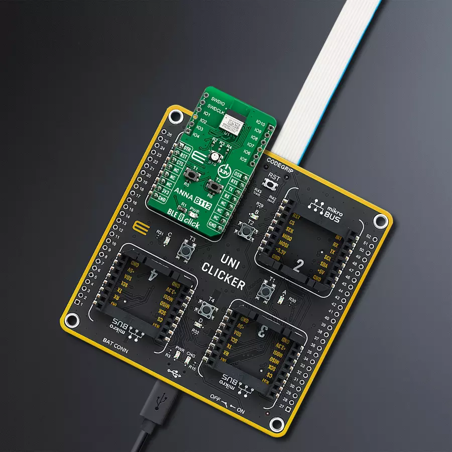
Click board™
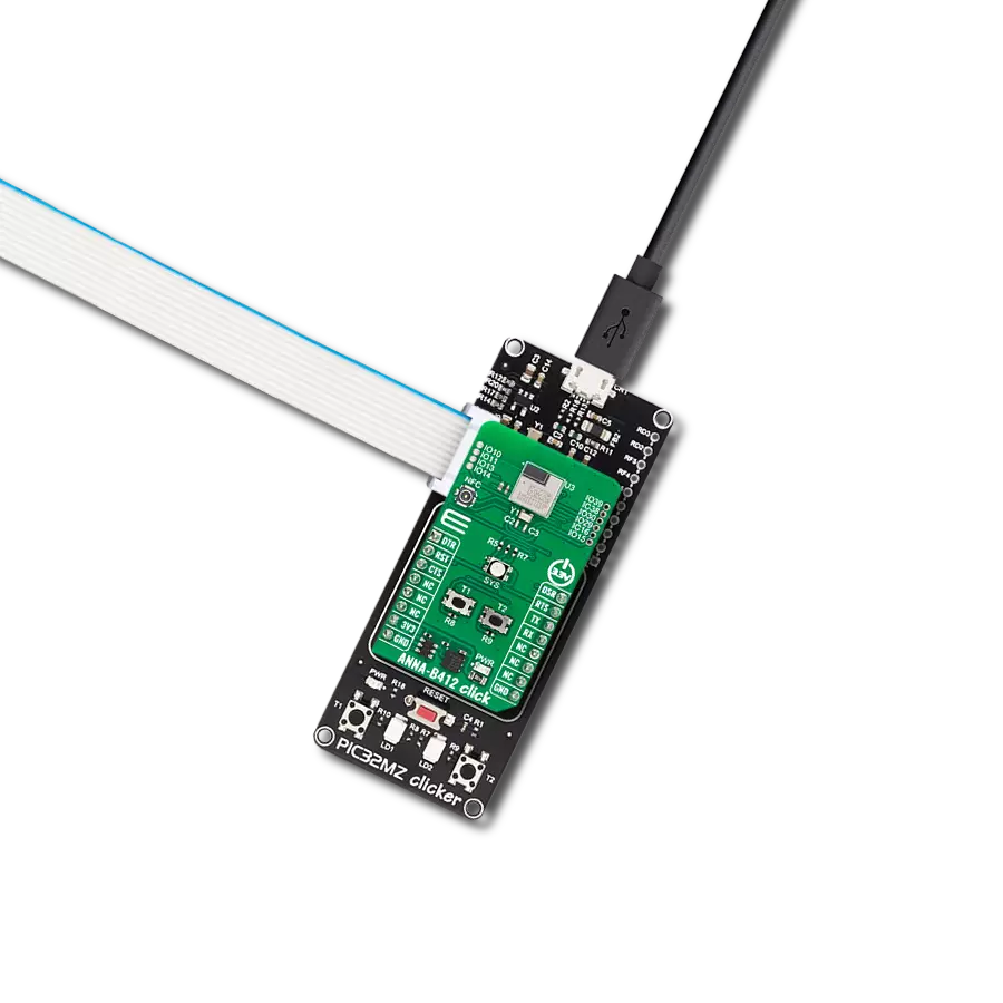
BLE 8 Click
Dev. board
UNI Clicker
Compiler
NECTO Studio
MCU
STM32F423RH
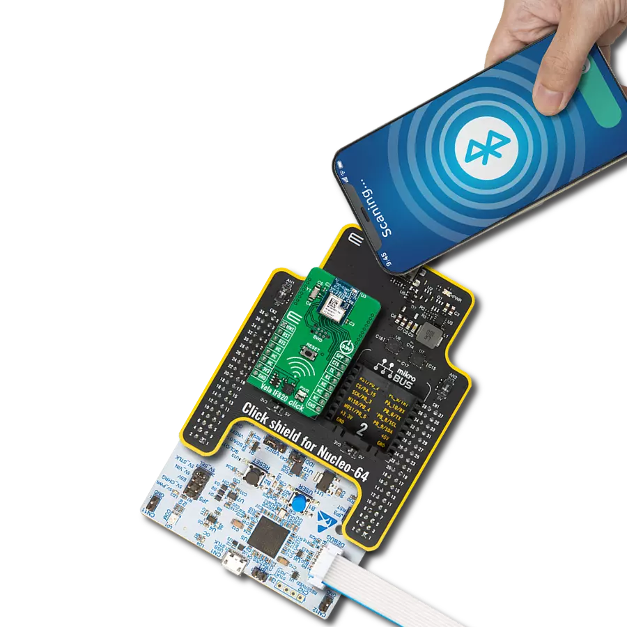
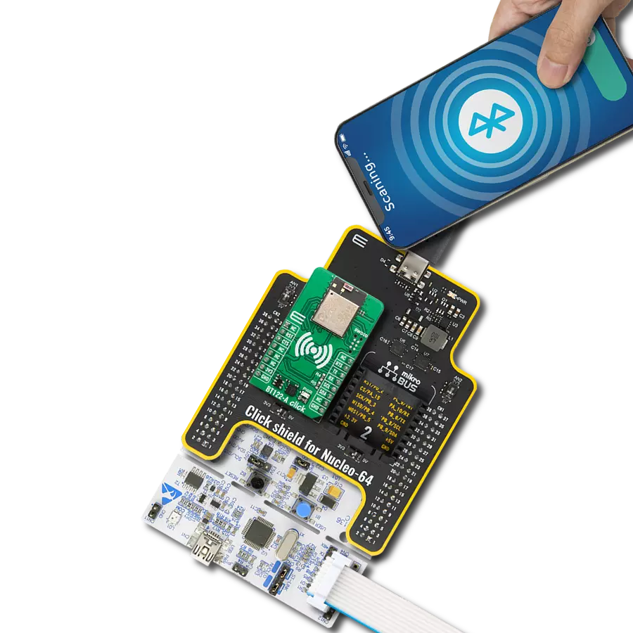
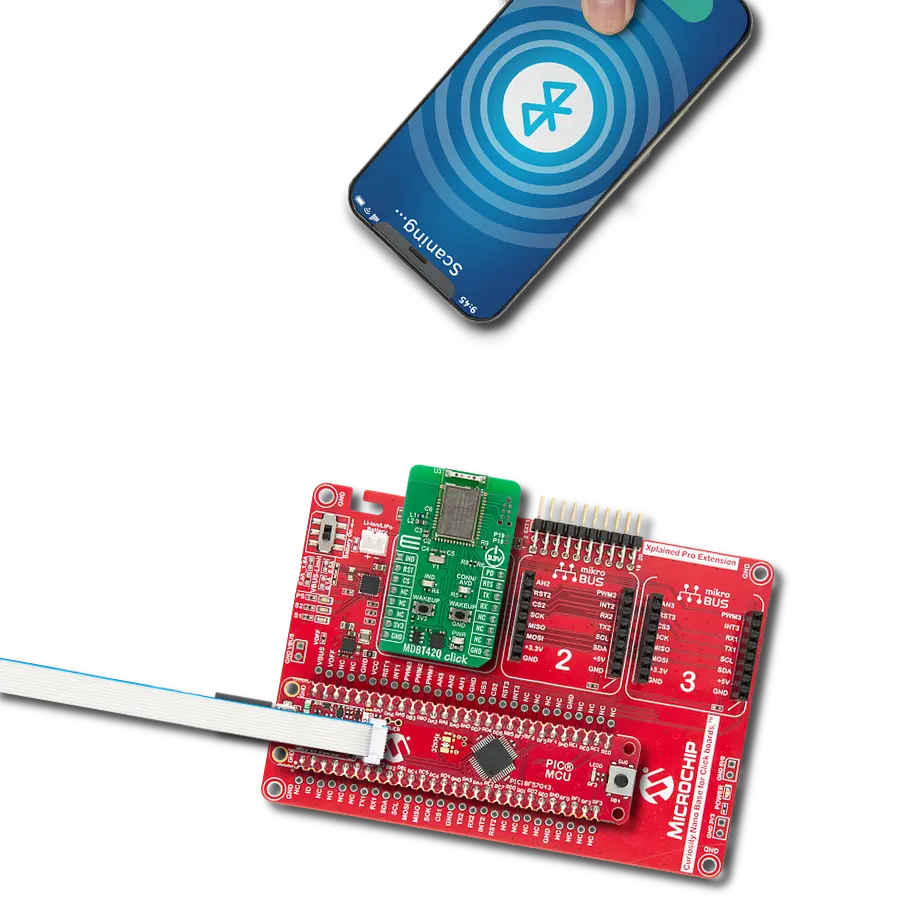
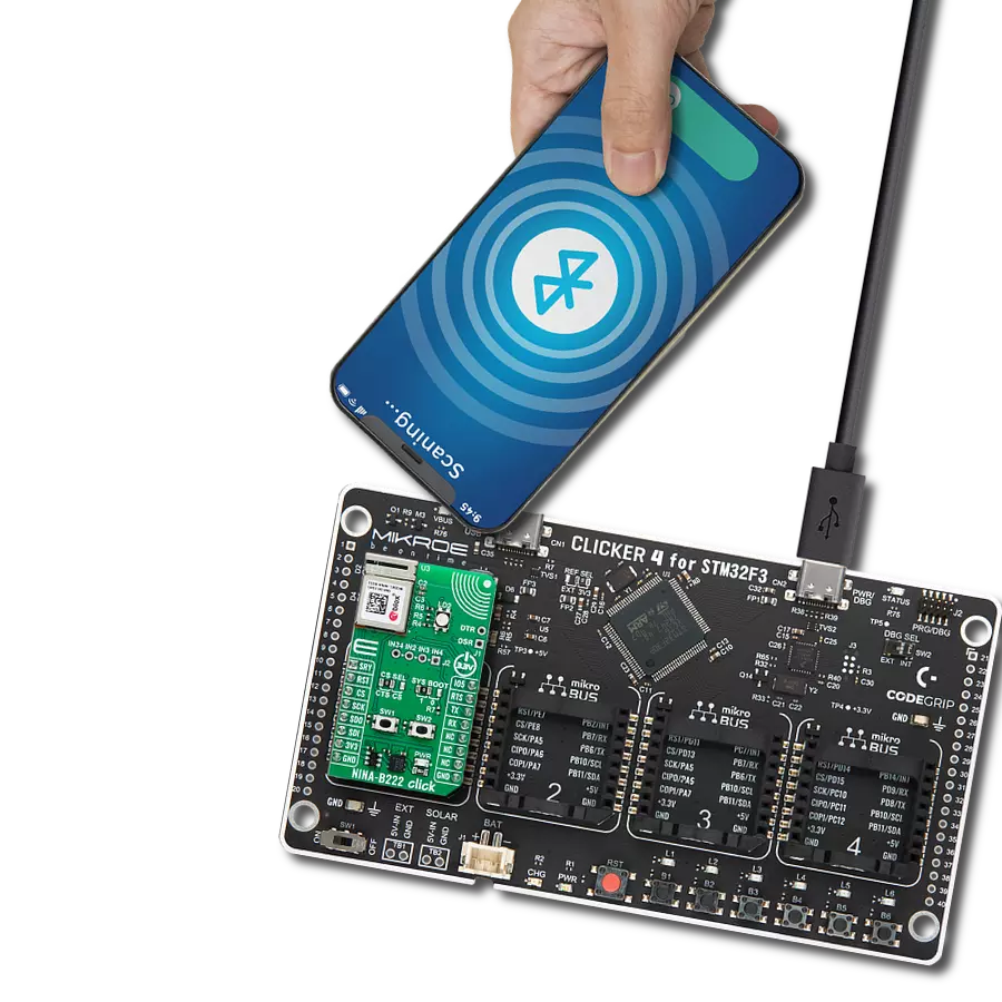
Our Bluetooth solution empowers you to enjoy wireless audio, transfer files, and interact with smart devices, all while experiencing unmatched reliability and efficiency
A
A
Hardware Overview
How does it work?
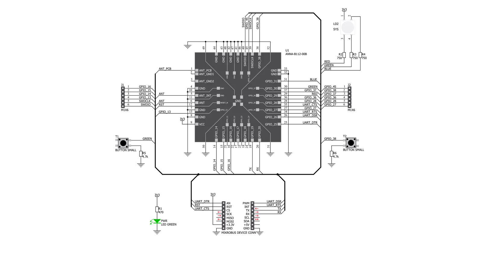
BLE 8 Click is based on the ANNA-B112, a standalone Bluetooth 5 low-energy module from u-blox based on the nRF52832 chip. The nRF52832 is the mid-range member of the nRF52 Series SoC family. It meets the challenges of a broad range of applications requiring Bluetooth 5 feature sets, protocol concurrency, and a rich and varied set of peripherals and features. In addition, it offers generous memory availability for both Flash and RAM. It is operated by a set of AT commands over the UART interface, which makes the BLE 8 click very easy to use. By integrating most of the critical components on the chip, the ANNA-B112 allows the module to overcome any imperfections of external discrete components, allowing signal transmission power of up to 5dBm, and -92 dBm
sensitivity for the receiver, using the on-chip antenna. The ANNA-B112 module is built around an ARM® Cortex™-M4 CPU with a floating point unit running at 64 MHz. It has NFC-A Tag for use in simplified pairing and payment solutions and numerous digital peripherals and interfaces, such as PDM and I2S, for digital microphones and audio. It is also fully multiprotocol capable with full protocol concurrency. It has protocol support for Bluetooth 5, Bluetooth mesh, ANT, and 2.4 GHz proprietary stacks. Besides the mikroBUS™ socket, BLE 8 click also features two optional 6-pin header mounts with marked pin labels. All of these pins can be externally connected and used for various purposes. SWDCLK and SWDIO pins are reserved for the SWD interface, which the ANNA-B112 series
modules use for flashing and debugging. The rest of the external pins, labeled as IO1-IO10, are general purpose IO type and can be programmed according to the users' needs. The onboard buttons T1 and T2 and the RGB, LED LD2 (labeled SYS) are also user programmable and can be used for various purposes for basic user interaction without any external components required besides the BLE 8 click. This Click board™ can be operated only with a 3.3V logic voltage level. The board must perform appropriate logic voltage level conversion before using MCUs with different logic levels. Also, it comes equipped with a library containing functions and an example code that can be used, as a reference, for further development.

Features overview
Development board
UNI Clicker is a compact development board designed as a complete solution that brings the flexibility of add-on Click boards™ to your favorite microcontroller, making it a perfect starter kit for implementing your ideas. It supports a wide range of microcontrollers, such as different ARM, PIC32, dsPIC, PIC, and AVR from various vendors like Microchip, ST, NXP, and TI (regardless of their number of pins), four mikroBUS™ sockets for Click board™ connectivity, a USB connector, LED indicators, buttons, a debugger/programmer connector, and two 26-pin headers for interfacing with external electronics. Thanks to innovative manufacturing technology, it allows you to build
gadgets with unique functionalities and features quickly. Each part of the UNI Clicker development kit contains the components necessary for the most efficient operation of the same board. In addition to the possibility of choosing the UNI Clicker programming method, using a third-party programmer or CODEGRIP/mikroProg connected to onboard JTAG/SWD header, the UNI Clicker board also includes a clean and regulated power supply module for the development kit. It provides two ways of board-powering; through the USB Type-C (USB-C) connector, where onboard voltage regulators provide the appropriate voltage levels to each component on the board, or using a Li-Po/Li
Ion battery via an onboard battery connector. All communication methods that mikroBUS™ itself supports are on this board (plus USB HOST/DEVICE), including the well-established mikroBUS™ socket, a standardized socket for the MCU card (SiBRAIN standard), and several user-configurable buttons and LED indicators. UNI Clicker is an integral part of the Mikroe ecosystem, allowing you to create a new application in minutes. Natively supported by Mikroe software tools, it covers many aspects of prototyping thanks to a considerable number of different Click boards™ (over a thousand boards), the number of which is growing every day.

Microcontroller Overview
MCU Card / MCU
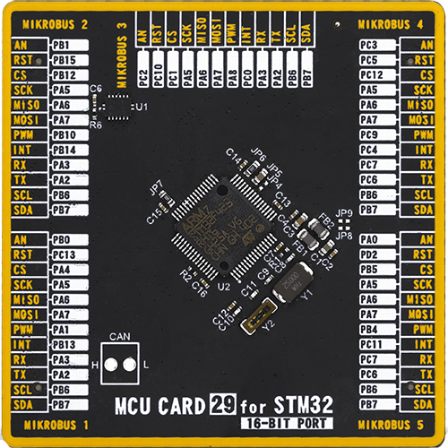
Type
8th Generation
Architecture
ARM Cortex-M4
MCU Memory (KB)
1536
Silicon Vendor
STMicroelectronics
Pin count
64
RAM (Bytes)
327680
Used MCU Pins
mikroBUS™ mapper
Take a closer look
Click board™ Schematic
Step by step
Project assembly

Start by selecting your development board and Click board™. Begin with the UNI Clicker as your development board.


Software Support
Library Description
This library contains API for BLE 8 Click driver.
Key functions:
ble8_reset- This function allows user to reset a module
Open Source
Code example
The complete application code and a ready-to-use project are available through the NECTO Studio Package Manager for direct installation in the NECTO Studio. The application code can also be found on the MIKROE GitHub account.
/*!
 * \file
 * \brief Ble8 Click example
 *
 * # Description
 * This example reads and processes data from BLE 8 Clicks.
 *
 * The demo application is composed of two sections :
 *
 * ## Application Init
 * Initializes driver and wake-up module.
 *
 * ## Application Task
 * Reads the received data.
 *
 * ## Additional Function
 * - ble8_process ( ) - Logs all received messages on UART, and sends the certain message back to the connected device.
 *
 * *note:*
 * <pre>
 * The all possible commands, module configuration and specification can be found in the
 * related documents:
 *     [1] ANNA-B112 System Integration Manual, document number UBX-18009821
 *     [2] u-blox Short Range AT Commands Manual, document number UBX-14044127
 *     [3] ANNA-B112 Getting Started Guide, document number UBX-18020387
 *     [4] ANNA-B112 Declaration of Conformity, document number UBX-18058993
 * </pre>
 *
 * \author MikroE Team
 *
 */
// ------------------------------------------------------------------- INCLUDES

#include "board.h"
#include "log.h"
#include "ble8.h"
#include "string.h"

#define PROCESS_COUNTER 5
#define PROCESS_RX_BUFFER_SIZE 100
#define PROCESS_PARSER_BUFFER_SIZE 100

// ------------------------------------------------------------------ VARIABLES

static ble8_t ble8;
static log_t logger;
static uint8_t data_mode = 0;

static char current_parser_buf[ PROCESS_PARSER_BUFFER_SIZE ];

// ------------------------------------------------------- ADDITIONAL FUNCTIONS

static int8_t ble8_process ( void )
{
    int32_t rsp_size;
    uint16_t rsp_cnt = 0;

    char uart_rx_buffer[ PROCESS_RX_BUFFER_SIZE ] = { 0 };
    uint8_t check_buf_cnt;
    uint8_t process_cnt = PROCESS_COUNTER;

    // Clear current buffer
    memset( current_parser_buf, 0, PROCESS_PARSER_BUFFER_SIZE );

    while( process_cnt != 0 )
    {
        rsp_size = ble8_generic_read( &ble8, uart_rx_buffer, PROCESS_RX_BUFFER_SIZE );

        if ( rsp_size > 0 )
        {
            // Validation of the received data
            for ( check_buf_cnt = 0; check_buf_cnt < rsp_size; check_buf_cnt++ )
            {
                if ( uart_rx_buffer[ check_buf_cnt ] == 0 )
                {
                    uart_rx_buffer[ check_buf_cnt ] = 13;
                }
            }
            // Storages data in current buffer
            rsp_cnt += rsp_size;
            if ( rsp_cnt < PROCESS_PARSER_BUFFER_SIZE )
            {
                strncat( current_parser_buf, uart_rx_buffer, rsp_size );
            }

            // Clear RX buffer
            memset( uart_rx_buffer, 0, PROCESS_RX_BUFFER_SIZE );

            if (strstr(current_parser_buf, "ERROR")) {
               return -1;
            }

            if (strstr(current_parser_buf, "OK")) {
               log_printf( &logger, "%s", current_parser_buf );
               Delay_100ms( );
               return 1;
            }

            if ( data_mode == 1) {
                log_printf( &logger, "%s", current_parser_buf );
                uart_write( &ble8.uart, "Hello", 5 );
                Delay_ms ( 1000 );
                Delay_ms ( 1000 );
                uart_write( &ble8.uart, "BLE8", 4 );
            }
        }
        else
        {
            process_cnt--;

            // Process delay
            Delay_ms ( 100 );
        }
    }

    return 0;
}

// ------------------------------------------------------ APPLICATION FUNCTIONS

void application_init ( void )
{
    log_cfg_t log_cfg;
    ble8_cfg_t cfg;

    /**
     * Logger initialization.
     * Default baud rate: 115200
     * Default log level: LOG_LEVEL_DEBUG
     * @note If USB_UART_RX and USB_UART_TX
     * are defined as HAL_PIN_NC, you will
     * need to define them manually for log to work.
     * See @b LOG_MAP_USB_UART macro definition for detailed explanation.
     */
    LOG_MAP_USB_UART( log_cfg );
    log_init( &logger, &log_cfg );
    log_info( &logger, "---- Application Init ----" );

    //  Click initialization.

    ble8_cfg_setup( &cfg );
    BLE8_MAP_MIKROBUS( cfg, MIKROBUS_1 );
    ble8_init( &ble8, &cfg );

    ble8_reset( &ble8 );
    Delay_1sec( );

    log_printf( &logger, "Configuring the module...\n" );
    Delay_1sec( );

    ble8_set_dsr_pin( &ble8, 1 );
    Delay_ms ( 20 );

    do {
        ble8_set_echo_cmd( &ble8, 1 );
        Delay_100ms( );
    }
    while( ble8_process( ) != 1 );

    do {
        ble8_set_local_name_cmd( &ble8, "BLE 8 Click" );
        Delay_100ms( );
    }
    while( ble8_process( ) != 1 );

    do {
        ble8_connectability_en_cmd( &ble8, BLE8_GAP_CONNECTABLE_MODE );
        Delay_100ms( );
    }
    while( ble8_process( ) != 1 );

    do {
        ble8_discoverability_en_cmd( &ble8, BLE8_GAP_GENERAL_DISCOVERABLE_MODE );
        Delay_100ms( );
    }
    while( ble8_process( ) != 1 );

    do {
        ble8_enter_mode_cmd( &ble8, BLE8_DATA_MODE );
        Delay_100ms( );
    }
    while( ble8_process( ) != 1 );

    ble8_set_dsr_pin( &ble8, 0 );
    Delay_ms ( 20 );
    data_mode = 1;
    log_printf( &logger, "The module has been configured.\n" );
}

void application_task ( void )
{
    ble8_process( );
}

int main ( void )
{
    /* Do not remove this line or clock might not be set correctly. */
    #ifdef PREINIT_SUPPORTED
    preinit();
    #endif

    application_init( );

    for ( ; ; )
    {
        application_task( );
    }

    return 0;
}


// ------------------------------------------------------------------------ END