Optimize pin utilization and reduce board complexity with CY8C9540A and STM32F303VE
Upgrade your I/O game!
Published Sep 23, 2023
Click board™
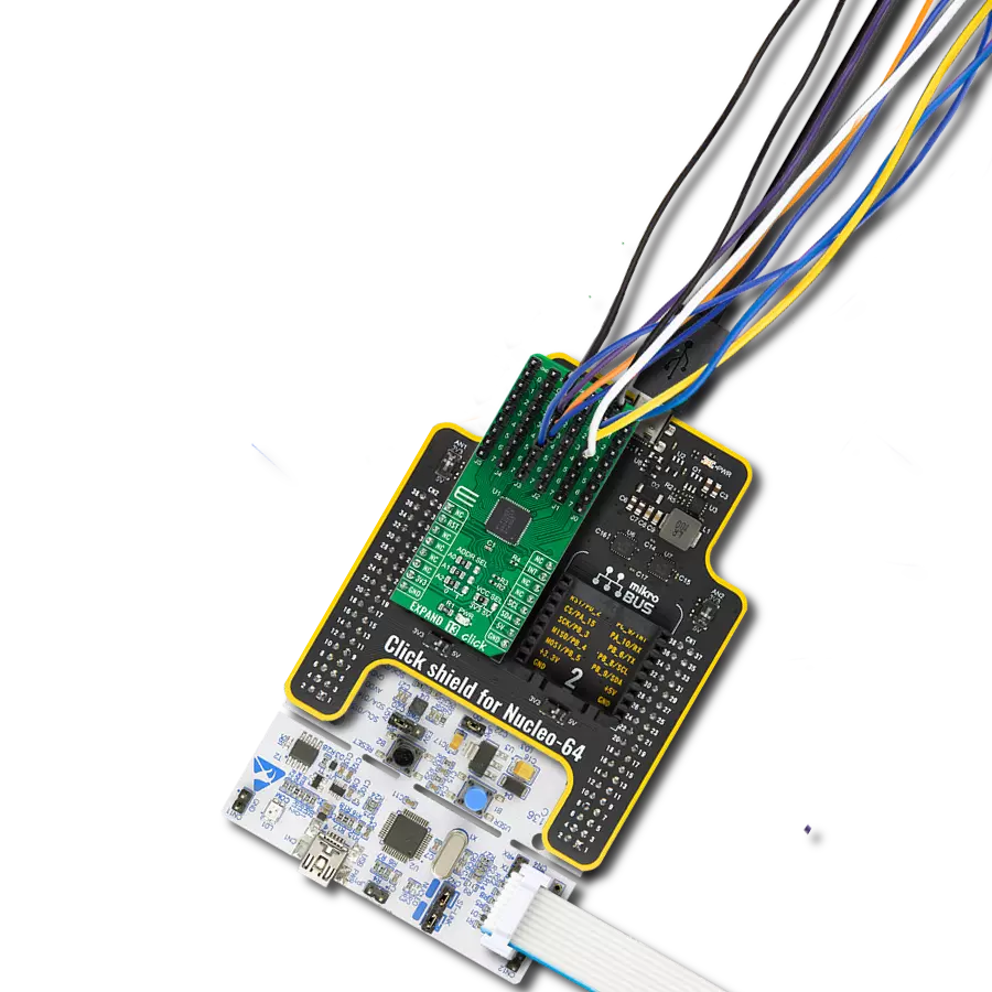
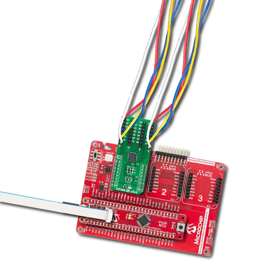
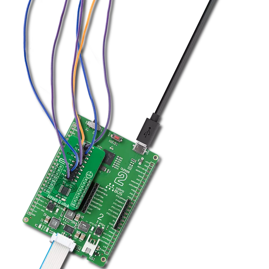
EXPAND 7 Click
Dev. board
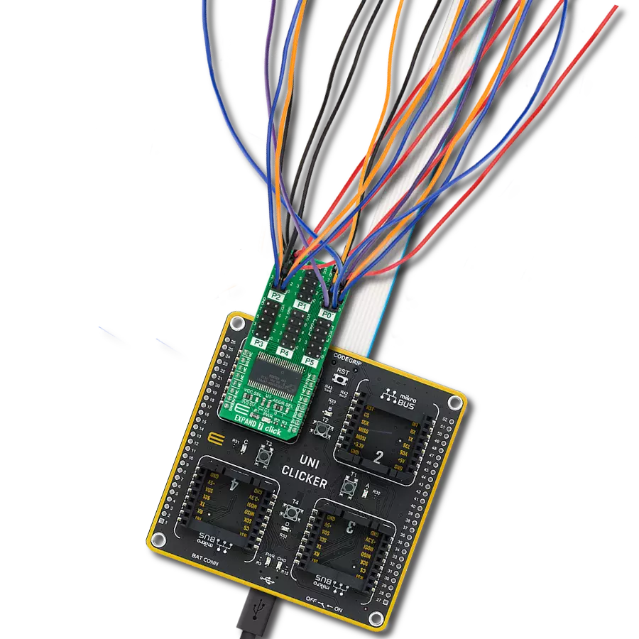
UNI Clicker
Compiler
NECTO Studio
MCU
STM32F303VE
Experience the versatility of our I/O pin expansion solution, tailored to provide you with the flexibility and control needed to optimize your projects, reduce complexity, and enhance connectivity
A
A
Hardware Overview
How does it work?
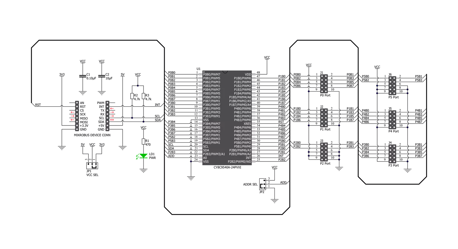
EXPAND 7 Click is based on the CY8C9540A, 40-bit I/O expander with EEPROM, and eight independently configurable 8-bit PWM outputs from Infineon. The main blocks of the CY8C9540A include the control unit, PWMs, EEPROM, and I/O ports. The I/O expander's data pins can be independently assigned as inputs, outputs, or PWM outputs and can be configured as open-drain or collector, strong drive (10 mA source, 25 mA sink), resistively pulled up or down, or high impedance which can be selected in the Port Drive Mode register. It operates as two I2C peripheral devices, where the first device is a multi-port I/O expander (single I2C address to access all ports through registers), and the second is a serial EEPROM with 11 Kbyte address space. Configuration and output register settings are storable as the user defaults in a dedicated section
of the EEPROM. If user defaults were stored in EEPROM, they are restored to the ports at the Power-Up sequence. The EEPROM is byte-readable and supports byte-by-byte writing. A pin 3 of Port 2 on this Click board™ can be configured as an EEPROM Write Disable (WD) input that blocks write operations when set high. The configuration registers can also turn off EEPROM operations. EXPAND 7 Click communicates with MCU using the standard I2C 2-Wire interface with a maximum frequency of 100kHz. The CY8C9540A has, by default, two possible I2C slave address formats: the first is used to access the multi-port device, and the second is to access the EEPROM. This selection of I2C slave addresses is performed by setting the logic level on the A0 pin of the CY8C9540A, which can be done using the SMD jumper labeled ADDR SEL. It also generates a
programmable interrupt signal routed on the INT pin of the mikroBUS™, which can inform the system master that there is incoming data on its ports or that the PWM output state has changed. The reset signal routed on the RST pin of the mikroBUS™ socket is similar to the POR (Power-ON Reset) function. When the CY8C9540A is held in Reset, all In and Out pins are held at their default High-Z State. This Click board™ can operate with either 3.3V or 5V logic voltage levels selected via the VCC SEL jumper. This way, both 3.3V and 5V capable MCUs can use the communication lines properly. Also, this Click board™ comes equipped with a library containing easy-to-use functions and an example code that can be used as a reference for further development.


Features overview
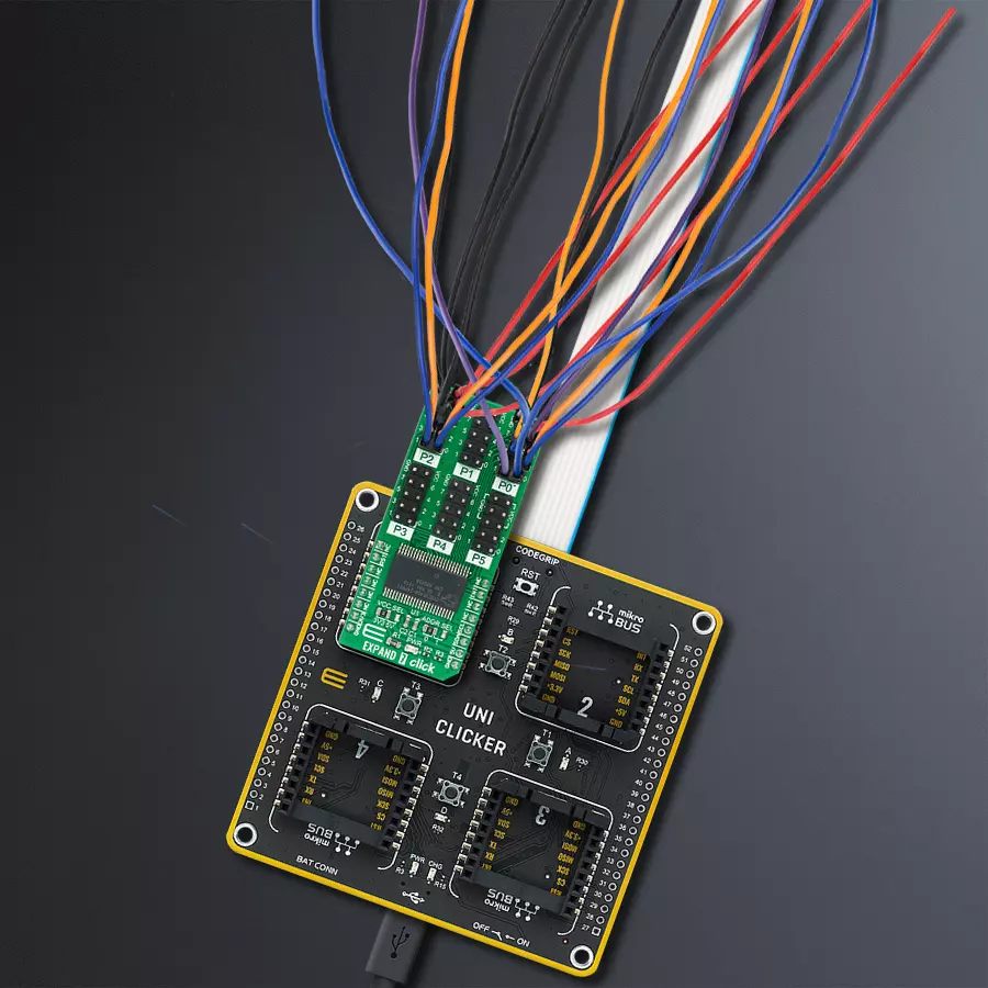
Development board
UNI Clicker is a compact development board designed as a complete solution that brings the flexibility of add-on Click boards™ to your favorite microcontroller, making it a perfect starter kit for implementing your ideas. It supports a wide range of microcontrollers, such as different ARM, PIC32, dsPIC, PIC, and AVR from various vendors like Microchip, ST, NXP, and TI (regardless of their number of pins), four mikroBUS™ sockets for Click board™ connectivity, a USB connector, LED indicators, buttons, a debugger/programmer connector, and two 26-pin headers for interfacing with external electronics. Thanks to innovative manufacturing technology, it allows you to build
gadgets with unique functionalities and features quickly. Each part of the UNI Clicker development kit contains the components necessary for the most efficient operation of the same board. In addition to the possibility of choosing the UNI Clicker programming method, using a third-party programmer or CODEGRIP/mikroProg connected to onboard JTAG/SWD header, the UNI Clicker board also includes a clean and regulated power supply module for the development kit. It provides two ways of board-powering; through the USB Type-C (USB-C) connector, where onboard voltage regulators provide the appropriate voltage levels to each component on the board, or using a Li-Po/Li
Ion battery via an onboard battery connector. All communication methods that mikroBUS™ itself supports are on this board (plus USB HOST/DEVICE), including the well-established mikroBUS™ socket, a standardized socket for the MCU card (SiBRAIN standard), and several user-configurable buttons and LED indicators. UNI Clicker is an integral part of the Mikroe ecosystem, allowing you to create a new application in minutes. Natively supported by Mikroe software tools, it covers many aspects of prototyping thanks to a considerable number of different Click boards™ (over a thousand boards), the number of which is growing every day.

Microcontroller Overview
MCU Card / MCU
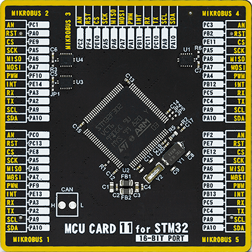
Type
8th Generation
Architecture
ARM Cortex-M4
MCU Memory (KB)
512
Silicon Vendor
STMicroelectronics
Pin count
100
RAM (Bytes)
81920
Used MCU Pins
mikroBUS™ mapper
Take a closer look
Click board™ Schematic
Step by step
Project assembly

Start by selecting your development board and Click board™. Begin with the UNI Clicker as your development board.


Software Support
Library Description
This library contains API for EXPAND 7 Click driver.
Key functions:
expand7_reset- Reset functionexpand7_write_all- Set all OUTPUT pins' logic levels functionexpand7_write_pin- Set a single OUTPUT pin's logic level function
Open Source
Code example
The complete application code and a ready-to-use project are available through the NECTO Studio Package Manager for direct installation in the NECTO Studio. The application code can also be found on the MIKROE GitHub account.
/*!
 * \file
 * \brief Expand7 Click example
 *
 * # Description
 * This example demonstrates the use of the EXPAND 7 Click.
 *
 * The demo application is composed of two sections :
 *
 * ## Application Init
 * Initalizes I2C driver and makes an initial log.
 *
 * ## Application Task
 * This example shows the capabilities of the EXPAND 7 Click by toggling
 * each of the 40 available pins.
 *
 * \author MikroE Team
 *
 */
// ------------------------------------------------------------------- INCLUDES

#include "board.h"
#include "log.h"
#include "expand7.h"

// ------------------------------------------------------------------ VARIABLES

static expand7_t expand7;
static log_t logger;

// ------------------------------------------------------ APPLICATION FUNCTIONS

void application_init ( void )
{
    log_cfg_t log_cfg;
    expand7_cfg_t cfg;

    /**
     * Logger initialization.
     * Default baud rate: 115200
     * Default log level: LOG_LEVEL_DEBUG
     * @note If USB_UART_RX and USB_UART_TX
     * are defined as HAL_PIN_NC, you will
     * need to define them manually for log to work.
     * See @b LOG_MAP_USB_UART macro definition for detailed explanation.
     */
    LOG_MAP_USB_UART( log_cfg );
    log_init( &logger, &log_cfg );
    log_info( &logger, "---- Application Init ----" );

    //  Click initialization.
    expand7_cfg_setup( &cfg );
    EXPAND7_MAP_MIKROBUS( cfg, MIKROBUS_1 );
    expand7_init( &expand7, &cfg );
    Delay_ms ( 100 );

    log_printf( &logger, "------------------- \r\n" );
    log_printf( &logger, "   EXPAND 7 Click   \r\n" );
    log_printf( &logger, "------------------- \r\n" );
}

void application_task ( void )
{
    expand7_write_all ( &expand7, 0xFF );
    log_printf( &logger, "All pins set to HIGH logic level!\r\n" );
    log_printf( &logger, "---------------------------------\r\n" );
    Delay_ms ( 1000 );
    Delay_ms ( 1000 );

    for ( uint8_t pin_num = 0; pin_num < 40; pin_num++ )
    {
        expand7_write_pin( &expand7, pin_num, EXPAND7_LOW );
        log_printf( &logger, "Pin %u is set to LOW logic level!\r\n", ( uint16_t ) pin_num );
        Delay_ms ( 300 );
    }
    log_printf( &logger, "---------------------------------\r\n" );
    Delay_ms ( 1000 );
}

int main ( void )
{
    /* Do not remove this line or clock might not be set correctly. */
    #ifdef PREINIT_SUPPORTED
    preinit();
    #endif

    application_init( );

    for ( ; ; )
    {
        application_task( );
    }

    return 0;
}

// ------------------------------------------------------------------------ END