Create digitally controlled oscillator with LTC6903 and STM32L4S5ZI
Timing perfection at your fingertips

Published May 27, 2023
Click board™
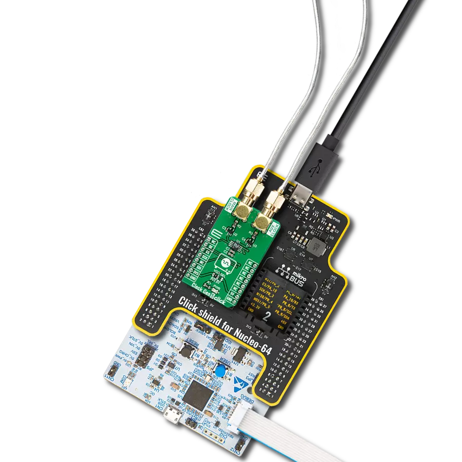
Clock Gen 5 Click
Dev. board
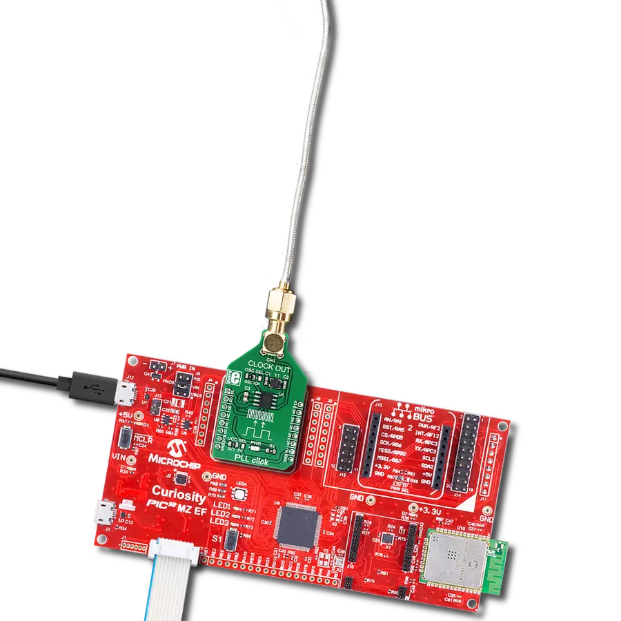
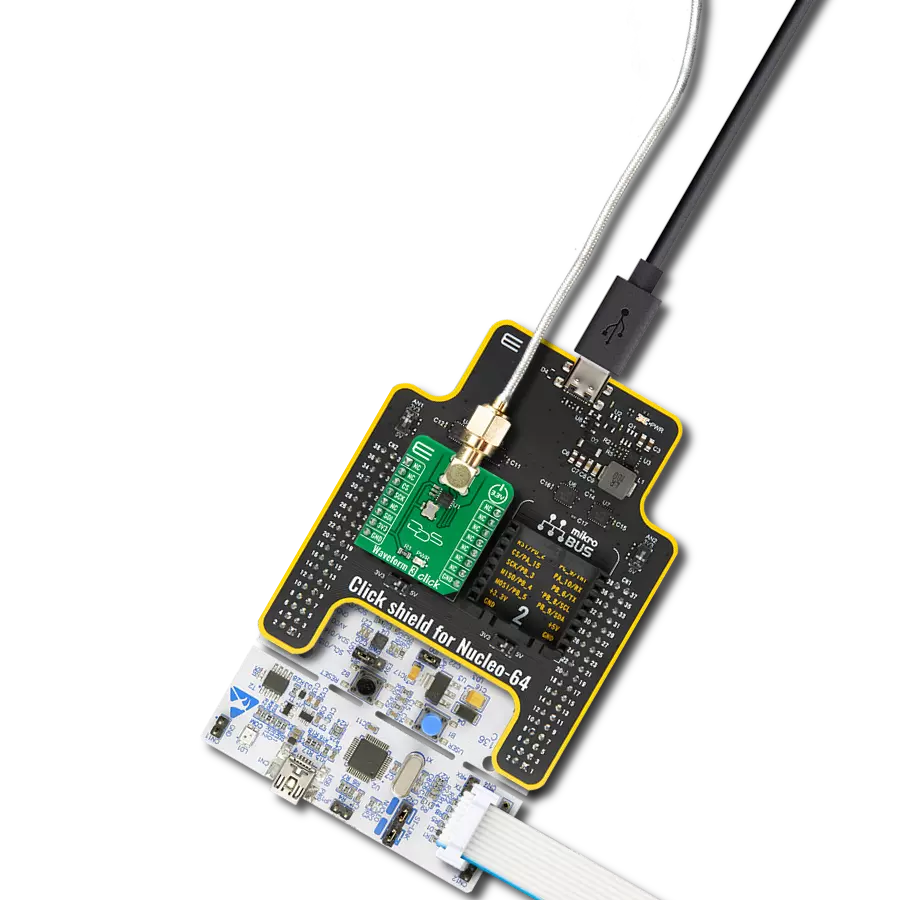
UNI Clicker
Compiler
NECTO Studio
MCU
STM32L4S5ZI
Elevate performance and maximize efficiency by adding a clock generator to your solution
A
A
Hardware Overview
How does it work?
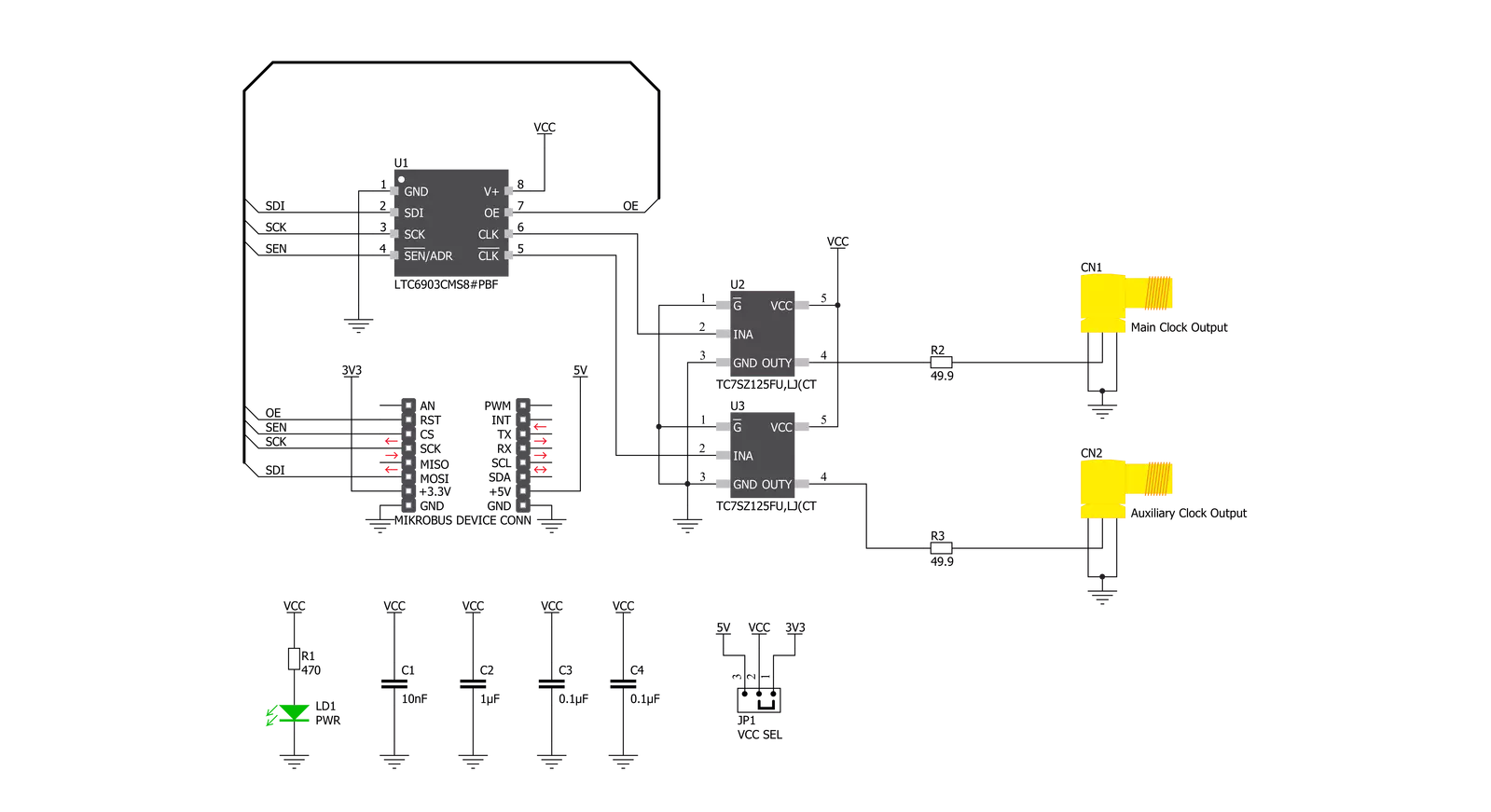
Clock Gen 5 Click is based on the LTC6903, a low-power self-contained digital frequency source providing a precision frequency from 1kHz to 68MHz set through a 3-wire digital interface from Analog Devices. The LTC6903 contains an internal feedback loop that controls a high-frequency square wave (VCO) operating between 34MHz and 68MHz. It is also a resistor-controlled oscillator that offers an integrated serial resistor DAC and a set of digital frequency dividers. The oscillator frequency is inversely proportional to the resistance of the DAC, where step size ranges between 0.05% and 0.1% of the frequency. In most frequency ranges, the output of the Clock Gen 5 Click is generated as a division of the higher internal clock
frequency. This helps to minimize jitter and sub-harmonics at the output of the device. In the highest frequency ranges, the division ratio is reduced, which will result in greater cycle-to-cycle jitter as well as spurs at the internal sampling frequency. The output clock signals, available on the SMA connectors with an impedance of 50Ω labeled as MAIN and AUX CLOCK, are primarily conducted through the TC7SZ125FU, a 3-state bus buffer before outputting allowing the LTC6903 to operate normally, producing the required output. Clock Gen 5 Click communicates with MCU using the 3-Wire SPI serial interface and operates at a clock frequency of up to 20 MHz. The output signals are controlled by the register bits MODE1 and MODE0,
where the outputs can be disabled through these bits. When both output signals are disabled through the mode control bits, the internal oscillator is also disabled. The OE pin routed on the RST pin of the mikroBUS™ socket can also be used to asynchronously disable either output without shutting down the oscillator entirely. This Click board™ can operate with either 3.3V or 5V logic voltage levels selected via the VCC SEL jumper. This way, both 3.3V and 5V capable MCUs can use the communication lines properly. However, the Click board™ comes equipped with a library containing easy-to-use functions and an example code that can be used, as a reference, for further development.


Features overview
Development board
UNI Clicker is a compact development board designed as a complete solution that brings the flexibility of add-on Click boards™ to your favorite microcontroller, making it a perfect starter kit for implementing your ideas. It supports a wide range of microcontrollers, such as different ARM, PIC32, dsPIC, PIC, and AVR from various vendors like Microchip, ST, NXP, and TI (regardless of their number of pins), four mikroBUS™ sockets for Click board™ connectivity, a USB connector, LED indicators, buttons, a debugger/programmer connector, and two 26-pin headers for interfacing with external electronics. Thanks to innovative manufacturing technology, it allows you to build
gadgets with unique functionalities and features quickly. Each part of the UNI Clicker development kit contains the components necessary for the most efficient operation of the same board. In addition to the possibility of choosing the UNI Clicker programming method, using a third-party programmer or CODEGRIP/mikroProg connected to onboard JTAG/SWD header, the UNI Clicker board also includes a clean and regulated power supply module for the development kit. It provides two ways of board-powering; through the USB Type-C (USB-C) connector, where onboard voltage regulators provide the appropriate voltage levels to each component on the board, or using a Li-Po/Li
Ion battery via an onboard battery connector. All communication methods that mikroBUS™ itself supports are on this board (plus USB HOST/DEVICE), including the well-established mikroBUS™ socket, a standardized socket for the MCU card (SiBRAIN standard), and several user-configurable buttons and LED indicators. UNI Clicker is an integral part of the Mikroe ecosystem, allowing you to create a new application in minutes. Natively supported by Mikroe software tools, it covers many aspects of prototyping thanks to a considerable number of different Click boards™ (over a thousand boards), the number of which is growing every day.

Microcontroller Overview
MCU Card / MCU
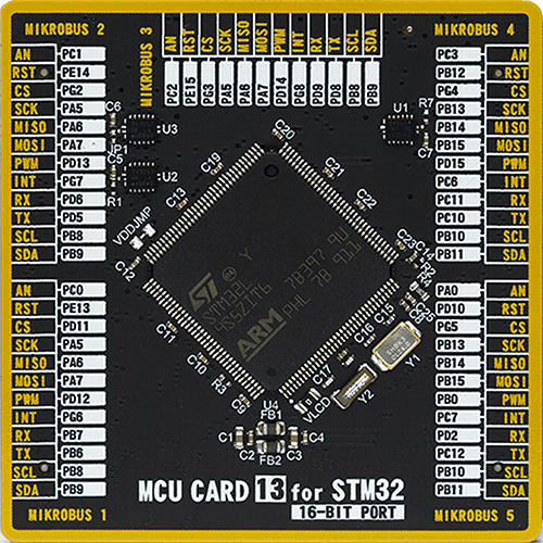
Type
8th Generation
Architecture
ARM Cortex-M4
MCU Memory (KB)
2048
Silicon Vendor
STMicroelectronics
Pin count
144
RAM (Bytes)
655360
Used MCU Pins
mikroBUS™ mapper
Take a closer look
Click board™ Schematic
Step by step
Project assembly

Start by selecting your development board and Click board™. Begin with the UNI Clicker as your development board.


Software Support
Library Description
This library contains API for Clock Gen 5 Click driver.
Key functions:
void clockgen5_out_enable ( uint8_t en_out )- Enable output function.void clockgen5_set_config ( uint8_t cfg )- Set configuration function.void clockgen5_set_freq ( float freq )- Set frequency function.
Open Source
Code example
The complete application code and a ready-to-use project are available through the NECTO Studio Package Manager for direct installation in the NECTO Studio. The application code can also be found on the MIKROE GitHub account.
/*!
 * @file main.c
 * @brief ClockGen5 Click example
 *
 * # Description
 * This is an example that demonstrates the use of the Clock Gen 5 Click board.
 *
 * The demo application is composed of two sections :
 *
 * ## Application Init
 * Initialization driver enables - SPI,
 * set output configuration CLK 180, also write log.
 *
 * ## Application Task
 * In this example, we adjusts different frequencies every 3 sec.
 * Results are being sent to the Uart Terminal where you can track their changes.
 *
 *
 * @author Stefan Ilic
 *
 */

#include "board.h"
#include "log.h"
#include "clockgen5.h"

static clockgen5_t clockgen5;
static log_t logger;

void application_init ( void ) {
    log_cfg_t log_cfg;  /**< Logger config object. */
    clockgen5_cfg_t clockgen5_cfg;  /**< Click config object. */

    /**
     * Logger initialization.
     * Default baud rate: 115200
     * Default log level: LOG_LEVEL_DEBUG
     * @note If USB_UART_RX and USB_UART_TX
     * are defined as HAL_PIN_NC, you will
     * need to define them manually for log to work.
     * See @b LOG_MAP_USB_UART macro definition for detailed explanation.
     */
    LOG_MAP_USB_UART( log_cfg );
    log_init( &logger, &log_cfg );
    log_info( &logger, " Application Init " );

    // Click initialization.

    clockgen5_cfg_setup( &clockgen5_cfg );
    CLOCKGEN5_MAP_MIKROBUS( clockgen5_cfg, MIKROBUS_1 );
    err_t init_flag  = clockgen5_init( &clockgen5, &clockgen5_cfg );
    if ( SPI_MASTER_ERROR == init_flag ) {
        log_error( &logger, " Application Init Error. " );
        log_info( &logger, " Please, run program again... %d", init_flag );

        for ( ; ; );
    }
    log_printf( &logger, "-----------------------\r\n" );
    log_printf( &logger, "    Enabling Output   \r\n" );
    clockgen5_out_enable( &clockgen5, CLOCKGEN5_OUTPUT_ENABLE);

    log_printf( &logger, "-----------------------\r\n" );
    log_printf( &logger, "   Set configuration   \r\n" );
    log_printf( &logger, "-----------------------\r\n" );
    clockgen5_set_config( &clockgen5, CLOCKGEN5_CFG_ON_CLK_180 );
    Delay_ms ( 500 );

    log_info( &logger, " Application Task " );
}

void application_task ( void ) {
    log_printf( &logger, "-----------------------\r\n" );
    log_printf( &logger, "        12.0 MHz       \r\n" );
    clockgen5_set_freq( &clockgen5, 12000.0 );
    Delay_ms ( 1000 );
    Delay_ms ( 1000 );
    Delay_ms ( 1000 );

    log_printf( &logger, "-----------------------\r\n" );
    log_printf( &logger, "         8.0 MHz       \r\n" );
    clockgen5_set_freq( &clockgen5, 8000.0 );
    Delay_ms ( 1000 );
    Delay_ms ( 1000 );
    Delay_ms ( 1000 );

    log_printf( &logger, "-----------------------\r\n" );
    log_printf( &logger, "         5.5 MHz       \r\n" );
    clockgen5_set_freq( &clockgen5, 5500.0 );
    Delay_ms ( 1000 );
    Delay_ms ( 1000 );
    Delay_ms ( 1000 );

    log_printf( &logger, "-----------------------\r\n" );
    log_printf( &logger, "         2.7 MHz       \r\n" );
    clockgen5_set_freq( &clockgen5, 2700.0 );
    Delay_ms ( 1000 );
    Delay_ms ( 1000 );
    Delay_ms ( 1000 );

    log_printf( &logger, "-----------------------\r\n" );
    log_printf( &logger, "         0.8 MHz       \r\n" );
    clockgen5_set_freq( &clockgen5, 800.0 );
    Delay_ms ( 1000 );
    Delay_ms ( 1000 );
    Delay_ms ( 1000 );

    log_printf( &logger, "-----------------------\r\n" );
    log_printf( &logger, "         0.2 MHz       \r\n" );
    clockgen5_set_freq( &clockgen5, 200.0 );
    Delay_ms ( 1000 );
    Delay_ms ( 1000 );
    Delay_ms ( 1000 );
}

int main ( void )
{
    /* Do not remove this line or clock might not be set correctly. */
    #ifdef PREINIT_SUPPORTED
    preinit();
    #endif

    application_init( );

    for ( ; ; )
    {
        application_task( );
    }

    return 0;
}

// ------------------------------------------------------------------------ END