Maintain power continuity and ensure optimal performance with TPS2115A and PIC18F47K42
Continuous power, Zero hassle: Experience seamless transition with us
Published Nov 01, 2023
Click board™
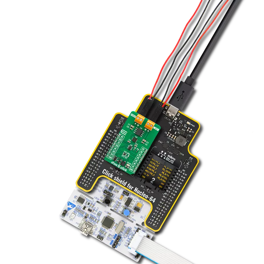
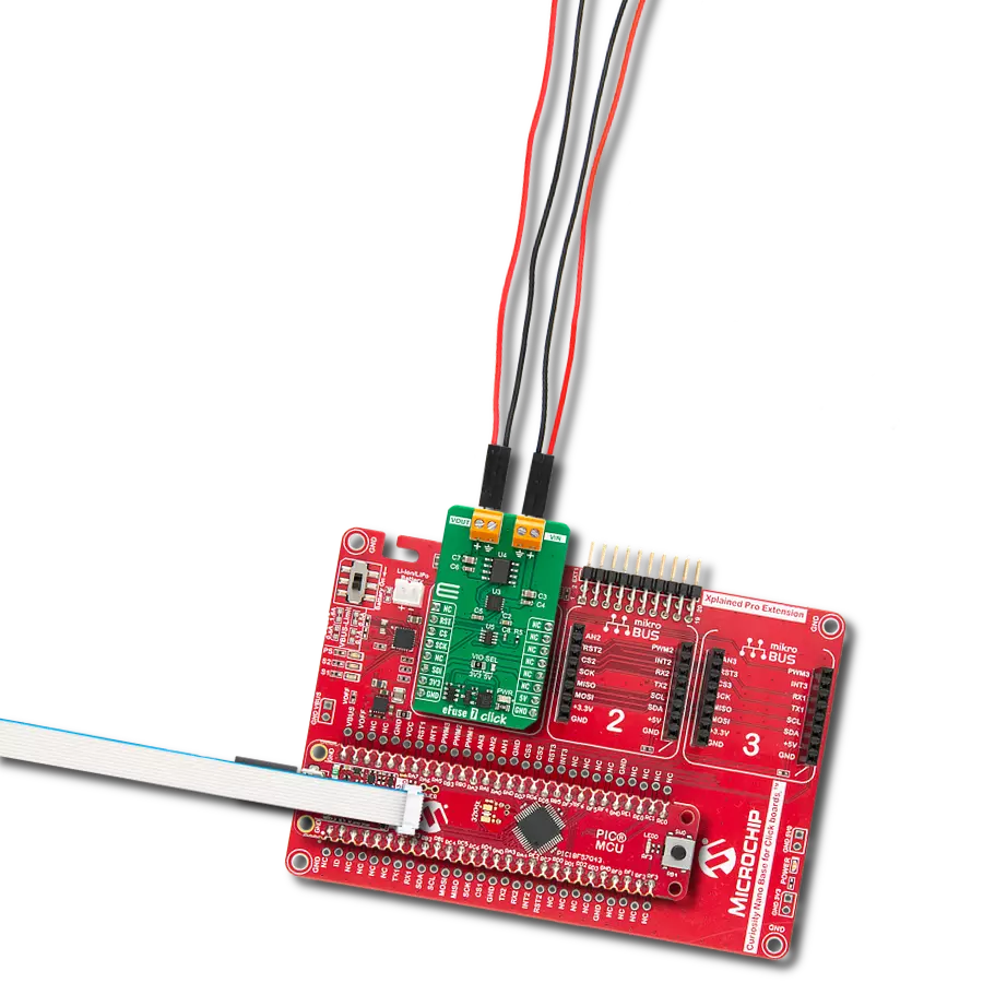
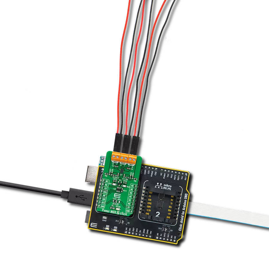
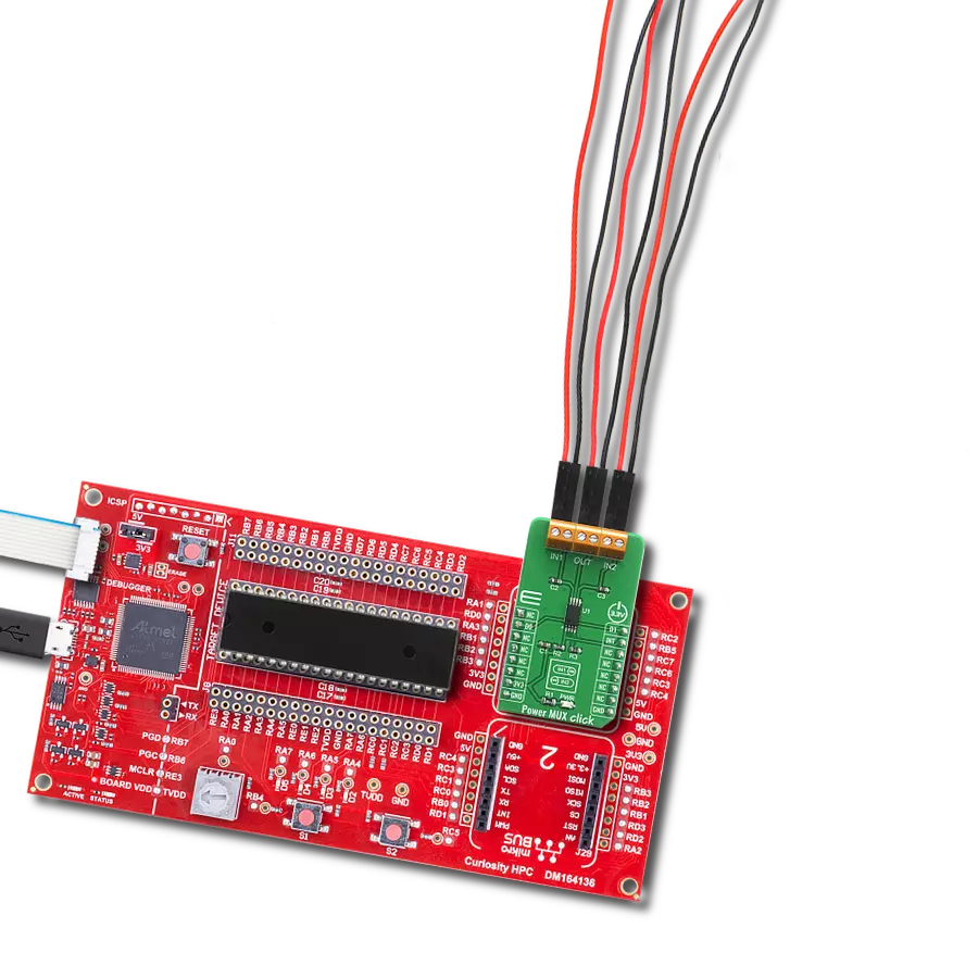
Power MUX Click
Dev. board
Curiosity HPC
Compiler
NECTO Studio
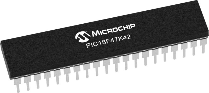
MCU
PIC18F47K42
Our power multiplexer is engineered to revolutionize the way your systems manage power, seamlessly transitioning between dual power sources for uninterrupted operation, even in the face of unexpected failures
A
A
Hardware Overview
How does it work?
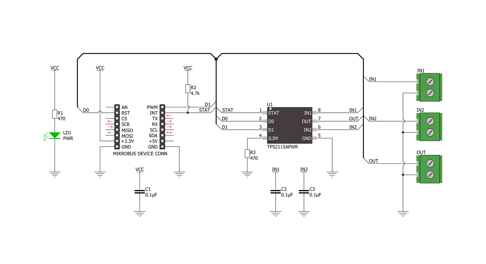
Power MUX Click is based on the TPS2115A, an auto-switching power multiplexer that enables transition between two power supplies, each operating at 2.8V to 5.5V voltage that comes from Texas Instruments. This Click board™ has two power switch inputs: primary and secondary. The IN1 switch can be enabled only if the IN1 supply is above the UVLO (under-voltage lockout) threshold, at least one supply exceeds the internal VDD UVLO, while the IN2 switch is enabled when the IN2 supply is above the UVLO threshold, and at least one supply exceeds the internal VDD UVLO. In auto-switching mode, pin D0 equals logic 1, and D1 pin equals logic 0, which means that this circuit will connect IN1 to OUT until the voltage at IN1 falls below a user-specified value. Once the voltage on IN1 falls below this value, the TPS2115A will select the higher of the two supplies. This usually means that the TPS2115A will swap to IN2. In manual
switching mode, pin D0 equals logic 0, and the multiplexer selects between two power supplies based on the D1 logic signal. OUT connects to IN1 if D1 is logic 1; otherwise, OUT connects to IN2. The logic thresholds for the D1 terminal are compatible with both TTL and CMOS logic. There is also interrupt pin STAT that is Hi-Z if the IN2 switch is ON, while STAT goes low if the IN1 switch is ON or OUT is Hi-Z. The under-voltage lockout circuit causes the output OUT to go Hi-Z if the selected power supply does not exceed the IN1/IN2 UVLO or if neither of the supplies exceeds the internal VDD UVLO. The switching circuitry ensures that both power switches will never conduct simultaneously. A comparator monitors the gate-to-source voltage of each power FET and allows an FET to turn ON only if the gate-to-source voltage of the other FET is below the turn-on threshold voltage. When the TPS2115A switches from a higher voltage supply
to a lower voltage supply, current can flow back from the load capacitor into the lower voltage supply. To minimize such reverse conduction, the TPS2115A will only connect a supply to the output once the output voltage has fallen to within 100 mV of the supply voltage. Once the supply has been connected to the output, it will remain connected regardless of the output voltage. This ensures the reliable operation of the IC and the Click board™ itself. Power MUX Click does not use the power from the mikroBUS™ power rails, except 3.3V for the LED indicator and interrupt‘s pull-up resistor. More information about the TPS2115A can be found in the attached datasheet. Also, this Click board™ comes equipped with a library containing easy-to-use functions and an example code that can be used as a reference for further development.

Features overview
Development board
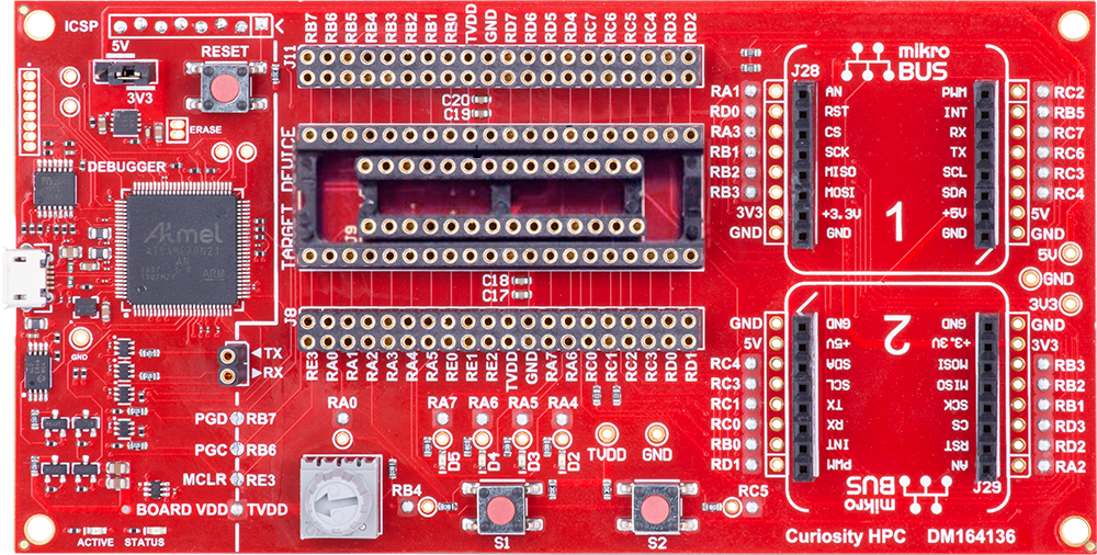
Curiosity HPC, standing for Curiosity High Pin Count (HPC) development board, supports 28- and 40-pin 8-bit PIC MCUs specially designed by Microchip for the needs of rapid development of embedded applications. This board has two unique PDIP sockets, surrounded by dual-row expansion headers, allowing connectivity to all pins on the populated PIC MCUs. It also contains a powerful onboard PICkit™ (PKOB), eliminating the need for an external programming/debugging tool, two mikroBUS™ sockets for Click board™ connectivity, a USB connector, a set of indicator LEDs, push button switches and a variable potentiometer. All
these features allow you to combine the strength of Microchip and Mikroe and create custom electronic solutions more efficiently than ever. Each part of the Curiosity HPC development board contains the components necessary for the most efficient operation of the same board. An integrated onboard PICkit™ (PKOB) allows low-voltage programming and in-circuit debugging for all supported devices. When used with the MPLAB® X Integrated Development Environment (IDE, version 3.0 or higher) or MPLAB® Xpress IDE, in-circuit debugging allows users to run, modify, and troubleshoot their custom software and hardware
quickly without the need for additional debugging tools. Besides, it includes a clean and regulated power supply block for the development board via the USB Micro-B connector, alongside all communication methods that mikroBUS™ itself supports. Curiosity HPC development board allows you to create a new application in just a few steps. Natively supported by Microchip software tools, it covers many aspects of prototyping thanks to many number of different Click boards™ (over a thousand boards), the number of which is growing daily.

Microcontroller Overview
MCU Card / MCU
Architecture
PIC
MCU Memory (KB)
128
Silicon Vendor
Microchip
Pin count
40
RAM (Bytes)
8192
Used MCU Pins
mikroBUS™ mapper
Take a closer look
Click board™ Schematic
Step by step
Project assembly
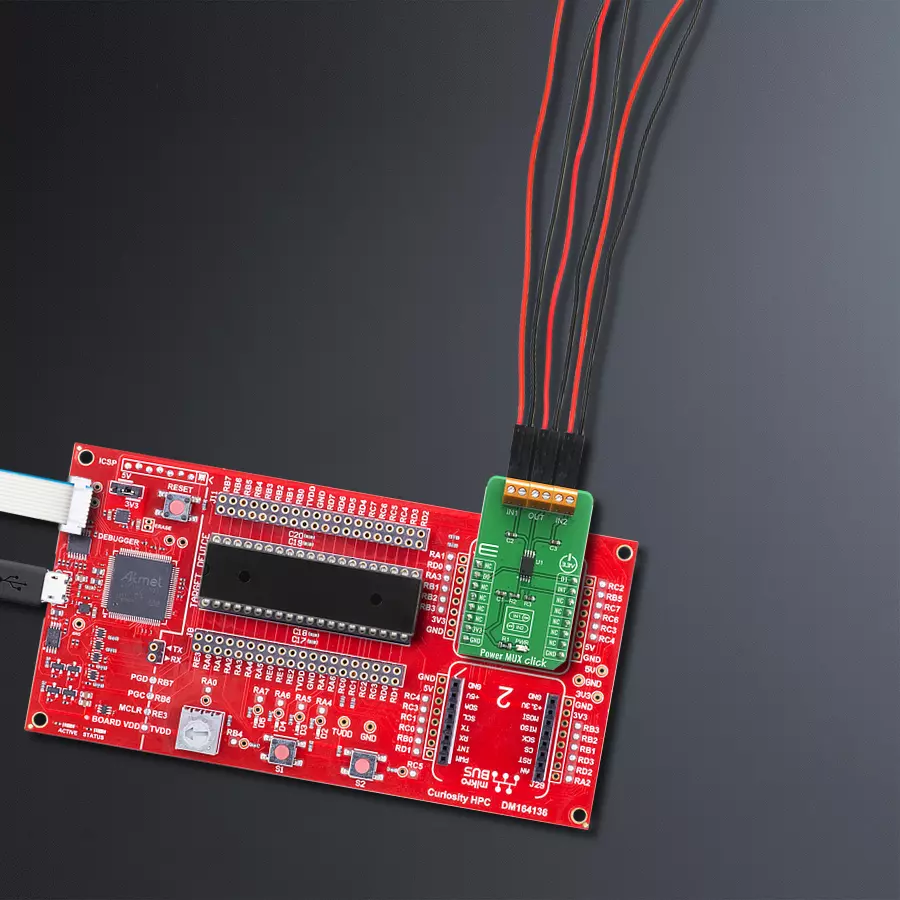
Start by selecting your development board and Click board™. Begin with the Curiosity HPC as your development board.


Track your results in real time
Application Output
1. Application Output - In Debug mode, the 'Application Output' window enables real-time data monitoring, offering direct insight into execution results. Ensure proper data display by configuring the environment correctly using the provided tutorial.

2. UART Terminal - Use the UART Terminal to monitor data transmission via a USB to UART converter, allowing direct communication between the Click board™ and your development system. Configure the baud rate and other serial settings according to your project's requirements to ensure proper functionality. For step-by-step setup instructions, refer to the provided tutorial.

3. Plot Output - The Plot feature offers a powerful way to visualize real-time sensor data, enabling trend analysis, debugging, and comparison of multiple data points. To set it up correctly, follow the provided tutorial, which includes a step-by-step example of using the Plot feature to display Click board™ readings. To use the Plot feature in your code, use the function: plot(*insert_graph_name*, variable_name);. This is a general format, and it is up to the user to replace 'insert_graph_name' with the actual graph name and 'variable_name' with the parameter to be displayed.

Software Support
Library Description
This library contains API for Power MUX Click driver.
Key functions:
powermux_int_pin_read- Power MUX pin reading functionpowermux_set_mode- Power MUX mode set function
Open Source
Code example
The complete application code and a ready-to-use project are available through the NECTO Studio Package Manager for direct installation in the NECTO Studio. The application code can also be found on the MIKROE GitHub account.
/*!
 * @file main.c
 * @brief Power MUX Click Example.
 *
 * # Description
 * This Click features power multiplexer that enables transition between two power supplies,
 * each operating at 2.8V to 5.5V and delivering up to 2A current depending on the package.
 *
 * The demo application is composed of two sections :
 *
 * ## Application Init
 * Enables GPIO and starts write log.
 *
 * ## Application Task
 * Changes power inputs every 3 seconds and displays the currently set mode on the USB UART.
 *
 * @author Mikroe Team
 *
 */

#include "board.h"
#include "log.h"
#include "powermux.h"

static powermux_t powermux;   /**< Power MUX Click driver object. */
static log_t logger;    /**< Logger object. */

void application_init ( void )
{
    log_cfg_t log_cfg;
    powermux_cfg_t powermux_cfg;

    /**
     * Logger initialization.
     * Default baud rate: 115200
     * Default log level: LOG_LEVEL_DEBUG
     * @note If USB_UART_RX and USB_UART_TX
     * are defined as HAL_PIN_NC, you will
     * need to define them manually for log to work.
     * See @b LOG_MAP_USB_UART macro definition for detailed explanation.
     */
    LOG_MAP_USB_UART( log_cfg );
    log_init( &logger, &log_cfg );
    log_info( &logger, " Application Init " );

    // Click initialization.
    powermux_cfg_setup( &powermux_cfg );
    POWERMUX_MAP_MIKROBUS( powermux_cfg, MIKROBUS_1 );
    if ( DIGITAL_OUT_UNSUPPORTED_PIN == powermux_init( &powermux, &powermux_cfg ) )
    {
        log_error( &logger, " Communication init." );
        for ( ; ; );
    }
    powermux_default_cfg ( &powermux );

    log_info( &logger, " Application Task " );
}

void application_task ( void )
{
    log_printf( &logger, " OUTPUT : IN1\r\n\n" );
    powermux_set_mode( &powermux, POWERMUX_INPUT_CHANNEL_1_ON );
    Delay_ms ( 1000 );
    Delay_ms ( 1000 );
    Delay_ms ( 1000 );
    log_printf( &logger, " OUTPUT : IN2\r\n\n" );
    powermux_set_mode( &powermux, POWERMUX_INPUT_CHANNEL_2_ON );
    Delay_ms ( 1000 );
    Delay_ms ( 1000 );
    Delay_ms ( 1000 );
    log_printf( &logger, " OUTPUT : OFF\r\n\n" );
    powermux_set_mode( &powermux, POWERMUX_INPUT_CHANNEL_OFF );
    Delay_ms ( 1000 );
    Delay_ms ( 1000 );
    Delay_ms ( 1000 );
    log_printf( &logger, " OUTPUT : AUTO\r\n\n" );
    powermux_set_mode( &powermux, POWERMUX_INPUT_CHANNEL_AUTO );
    Delay_ms ( 1000 );
    Delay_ms ( 1000 );
    Delay_ms ( 1000 );
}

int main ( void )
{
    /* Do not remove this line or clock might not be set correctly. */
    #ifdef PREINIT_SUPPORTED
    preinit();
    #endif

    application_init( );

    for ( ; ; )
    {
        application_task( );
    }

    return 0;
}

// ------------------------------------------------------------------------ END
Additional Support
Resources
Category:Power Switch