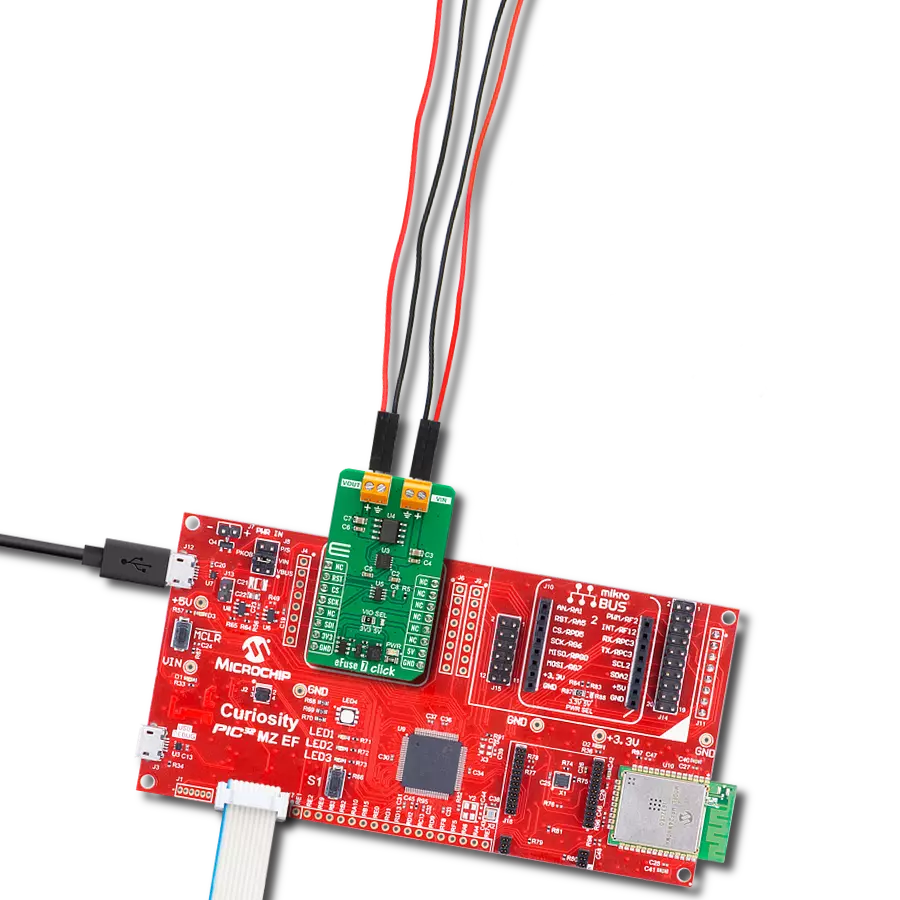
Control the flow of power to connected loads (resistive, inductive, and capacitive) with with BV2HD070EFU-C and PIC18F57Q43
AEC-Q100 qualified (Grade 1) two-channel high-side switch for controlling various loads

Published Dec 11, 2024
Click board™
IPD 2 Click
Dev. board
Curiosity Nano with PIC18F57Q43
Compiler
NECTO Studio
MCU
PIC18F57Q43
High-side switching with advanced protection and diagnostics perfect for automotive lighting, motor control, and solenoid applications
A
A
Hardware Overview
How does it work?
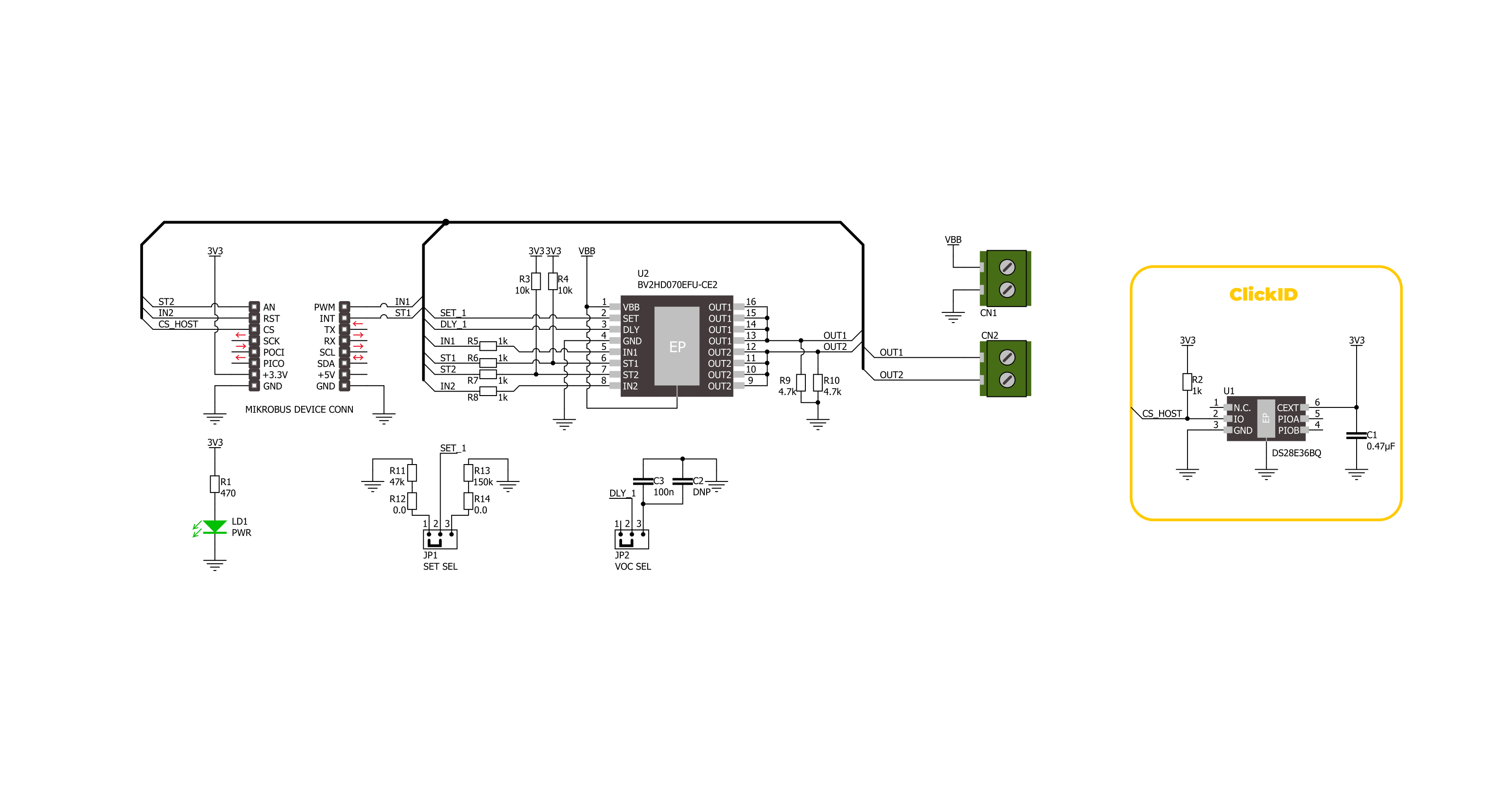
IPD 2 Click is based on the BV2HD070EFU-C, an automotive-grade two-channel high-side switch from ROHM Semiconductor, designed to handle resistive, inductive, and capacitive loads in automotive applications. The BV2HD070EFU-C features a 70mΩ on-resistance high-side switch and incorporates advanced protection and diagnostic functionalities to ensure reliable operation in demanding environments. This Click board™ is particularly suitable for automotive applications, supporting various types of loads such as lights, solenoids, and motors. It provides an efficient, reliable, and compact solution for high-side switching requirements, ensuring stable performance and enhanced safety in automotive systems. The BV2HD070EFU-C is AEC-Q100 qualified (Grade 1) and operates across a wide input voltage range of 6V to 28V, supplied via the VDD terminal. Its comprehensive protection suite includes overcurrent detection (OCD) with a
configurable mask function, ensuring precise fault management and preventing unintended load disconnection. Additional safety features include thermal shutdown protection, which halts operation under excessive temperature conditions, and undervoltage lockout (UVLO) to safeguard against unstable power supply conditions. Moreover, the switch includes an open load detection function, providing feedback when the load is disconnected or the circuit is incomplete. This Click board™ uses several pins of the mikroBUS™ socket for control and diagnostics. The IN1 and IN2 pins serve as control signals, enabling activation of the respective outputs marked as 1 and 2 on the output OUT terminal. For monitoring and fault detection, the board includes a diagnostic output function accessible via the ST1 and ST2 pins of the mikroBUS™ socket, providing real-time feedback on abnormalities. In addition to these control and diagnostic pins, the board features two
configuration jumpers. The first, SET SEL, allows users to configure the overcurrent limit between 1A and the default value of 2.3A. While the BV2HD070EFU-C supports overcurrent limits of up to approximately 10A, users can achieve this by replacing the selected resistance as specified in the datasheet recommendations. The second jumper, VOC SEL, activates a functionality that optimizes the time required to achieve precise overcurrent protection for the connected load. This feature is enabled by default, ensuring enhanced load safety and performance without additional configuration. This Click board™ can be operated only with a 3.3V logic voltage level. The board must perform appropriate logic voltage level conversion before using MCUs with different logic levels. It also comes equipped with a library containing functions and example code that can be used as a reference for further development.

Features overview
Development board
PIC18F57Q43 Curiosity Nano evaluation kit is a cutting-edge hardware platform designed to evaluate microcontrollers within the PIC18-Q43 family. Central to its design is the inclusion of the powerful PIC18F57Q43 microcontroller (MCU), offering advanced functionalities and robust performance. Key features of this evaluation kit include a yellow user LED and a responsive
mechanical user switch, providing seamless interaction and testing. The provision for a 32.768kHz crystal footprint ensures precision timing capabilities. With an onboard debugger boasting a green power and status LED, programming and debugging become intuitive and efficient. Further enhancing its utility is the Virtual serial port (CDC) and a debug GPIO channel (DGI
GPIO), offering extensive connectivity options. Powered via USB, this kit boasts an adjustable target voltage feature facilitated by the MIC5353 LDO regulator, ensuring stable operation with an output voltage ranging from 1.8V to 5.1V, with a maximum output current of 500mA, subject to ambient temperature and voltage constraints.

Microcontroller Overview
MCU Card / MCU

Architecture
PIC
MCU Memory (KB)
128
Silicon Vendor
Microchip
Pin count
48
RAM (Bytes)
8196
You complete me!
Accessories
Curiosity Nano Base for Click boards is a versatile hardware extension platform created to streamline the integration between Curiosity Nano kits and extension boards, tailored explicitly for the mikroBUS™-standardized Click boards and Xplained Pro extension boards. This innovative base board (shield) offers seamless connectivity and expansion possibilities, simplifying experimentation and development. Key features include USB power compatibility from the Curiosity Nano kit, alongside an alternative external power input option for enhanced flexibility. The onboard Li-Ion/LiPo charger and management circuit ensure smooth operation for battery-powered applications, simplifying usage and management. Moreover, the base incorporates a fixed 3.3V PSU dedicated to target and mikroBUS™ power rails, alongside a fixed 5.0V boost converter catering to 5V power rails of mikroBUS™ sockets, providing stable power delivery for various connected devices.

Used MCU Pins
mikroBUS™ mapper
Take a closer look
Click board™ Schematic
Step by step
Project assembly

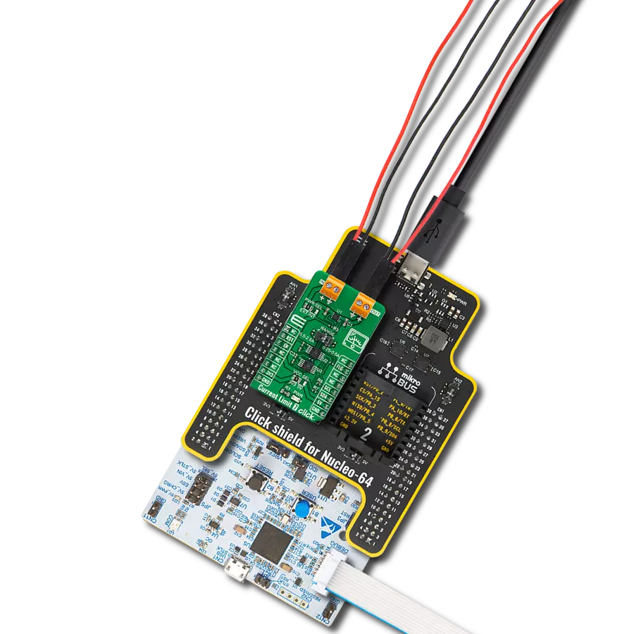
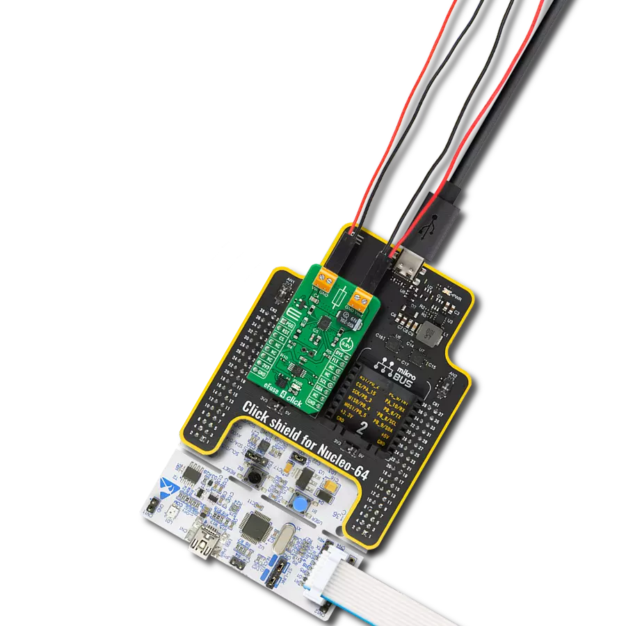
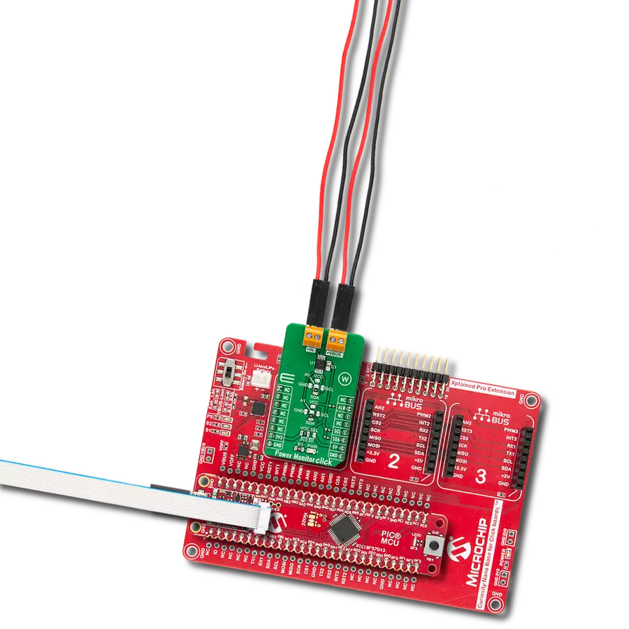
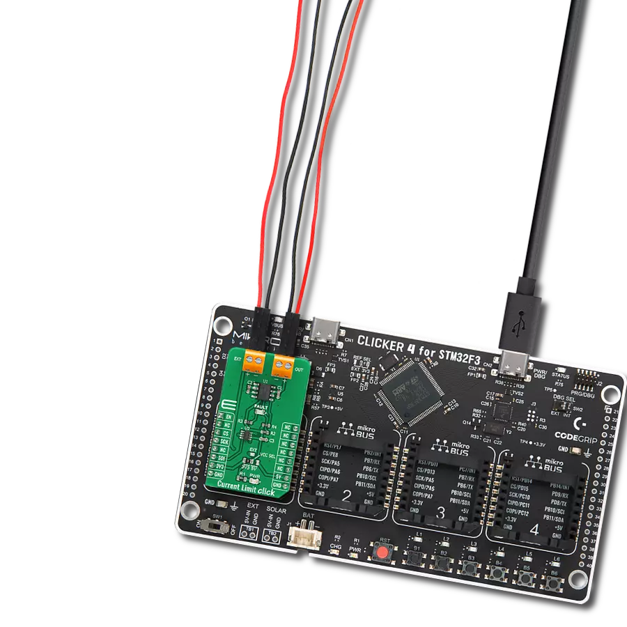
Start by selecting your development board and Click board™. Begin with the Curiosity Nano with PIC18F57Q43 as your development board.


Software Support
Library Description
This library contains API for IPD 2 Click driver.
Key functions:
ipd2_enable_out1- This function enables OUT1 by setting the IN1 pin to high logic state.ipd2_disable_out1- This function disables OUT1 by setting the IN1 pin to low logic state.ipd2_get_st1_pin- This function returns the ST1 pin logic state.
Open Source
Code example
The complete application code and a ready-to-use project are available through the NECTO Studio Package Manager for direct installation in the NECTO Studio. The application code can also be found on the MIKROE GitHub account.
/*!
 * @file main.c
 * @brief IPD 2 Click Example.
 *
 * # Description
 * This example demonstrates the use of IPD 2 Click by toggling the output state.
 *
 * The demo application is composed of two sections :
 *
 * ## Application Init
 * Initializes the driver and logger.
 *
 * ## Application Task
 * Toggles OUT1 and OUT2 state every 3 seconds and displays both outputs state and
 * status diagnostics pin state. If the status pin is HIGH it indicates that the fault
 * condition on this output has occurred and the output is disabled.
 *
 * @author Stefan Filipovic
 *
 */

#include "board.h"
#include "log.h"
#include "ipd2.h"

static ipd2_t ipd2;     /**< IPD 2 Click driver object. */
static log_t logger;    /**< Logger object. */

void application_init ( void )
{
    log_cfg_t log_cfg;  /**< Logger config object. */
    ipd2_cfg_t ipd2_cfg;  /**< Click config object. */

    /**
     * Logger initialization.
     * Default baud rate: 115200
     * Default log level: LOG_LEVEL_DEBUG
     * @note If USB_UART_RX and USB_UART_TX
     * are defined as HAL_PIN_NC, you will
     * need to define them manually for log to work.
     * See @b LOG_MAP_USB_UART macro definition for detailed explanation.
     */
    LOG_MAP_USB_UART( log_cfg );
    log_init( &logger, &log_cfg );
    log_info( &logger, " Application Init " );

    // Click initialization.
    ipd2_cfg_setup( &ipd2_cfg );
    IPD2_MAP_MIKROBUS( ipd2_cfg, MIKROBUS_1 );
    if ( DIGITAL_OUT_UNSUPPORTED_PIN == ipd2_init( &ipd2, &ipd2_cfg ) )
    {
        log_error( &logger, " Communication init." );
        for ( ; ; );
    }

    log_info( &logger, " Application Task " );
}

void application_task ( void )
{
    ipd2_enable_out1 ( &ipd2 );
    ipd2_disable_out2 ( &ipd2 );
    Delay_ms ( 100 );
    log_printf( &logger, " OUT1: enabled\r\n" );
    log_printf( &logger, " OUT2: disabled\r\n" );
    log_printf( &logger, " ST1: %s\r\n", ( char * ) ( ipd2_get_st1_pin ( &ipd2 ) ? "high" : "low" ) );
    log_printf( &logger, " ST2: %s\r\n\n", ( char * ) ( ipd2_get_st2_pin ( &ipd2 ) ? "high" : "low" ) );
    Delay_ms ( 1000 );
    Delay_ms ( 1000 );
    Delay_ms ( 1000 );

    ipd2_disable_out1 ( &ipd2 );
    ipd2_enable_out2 ( &ipd2 );
    Delay_ms ( 100 );
    log_printf( &logger, " OUT1: disabled\r\n" );
    log_printf( &logger, " OUT2: enabled\r\n" );
    log_printf( &logger, " ST1: %s\r\n", ( char * ) ( ipd2_get_st1_pin ( &ipd2 ) ? "high" : "low" ) );
    log_printf( &logger, " ST2: %s\r\n\n", ( char * ) ( ipd2_get_st2_pin ( &ipd2 ) ? "high" : "low" ) );
    Delay_ms ( 1000 );
    Delay_ms ( 1000 );
    Delay_ms ( 1000 );
}

int main ( void )
{
    /* Do not remove this line or clock might not be set correctly. */
    #ifdef PREINIT_SUPPORTED
    preinit();
    #endif

    application_init( );

    for ( ; ; )
    {
        application_task( );
    }

    return 0;
}

// ------------------------------------------------------------------------ END
Additional Support
Resources
Category:Power Switch