Achieve stable connection between high-voltage components and low-voltage equipment using TLP2770 and PIC32MZ2048EFM100
Optocouplers: Where light and data high-five

Published Sep 21, 2023
Click board™
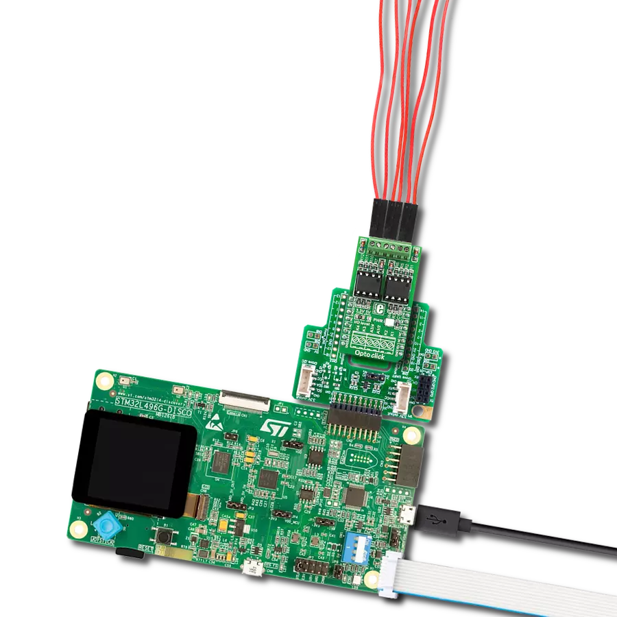
Opto 2 Click
Dev. board
Curiosity PIC32 MZ EF
Compiler
NECTO Studio
MCU
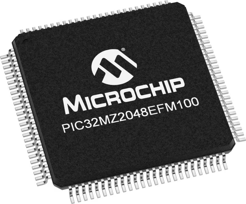
PIC32MZ2048EFM100
Safeguard delicate signals from potential harm, such as electrical noise or voltage fluctuations, ensuring they reach their destination intact and unaltered.
A
A
Hardware Overview
How does it work?
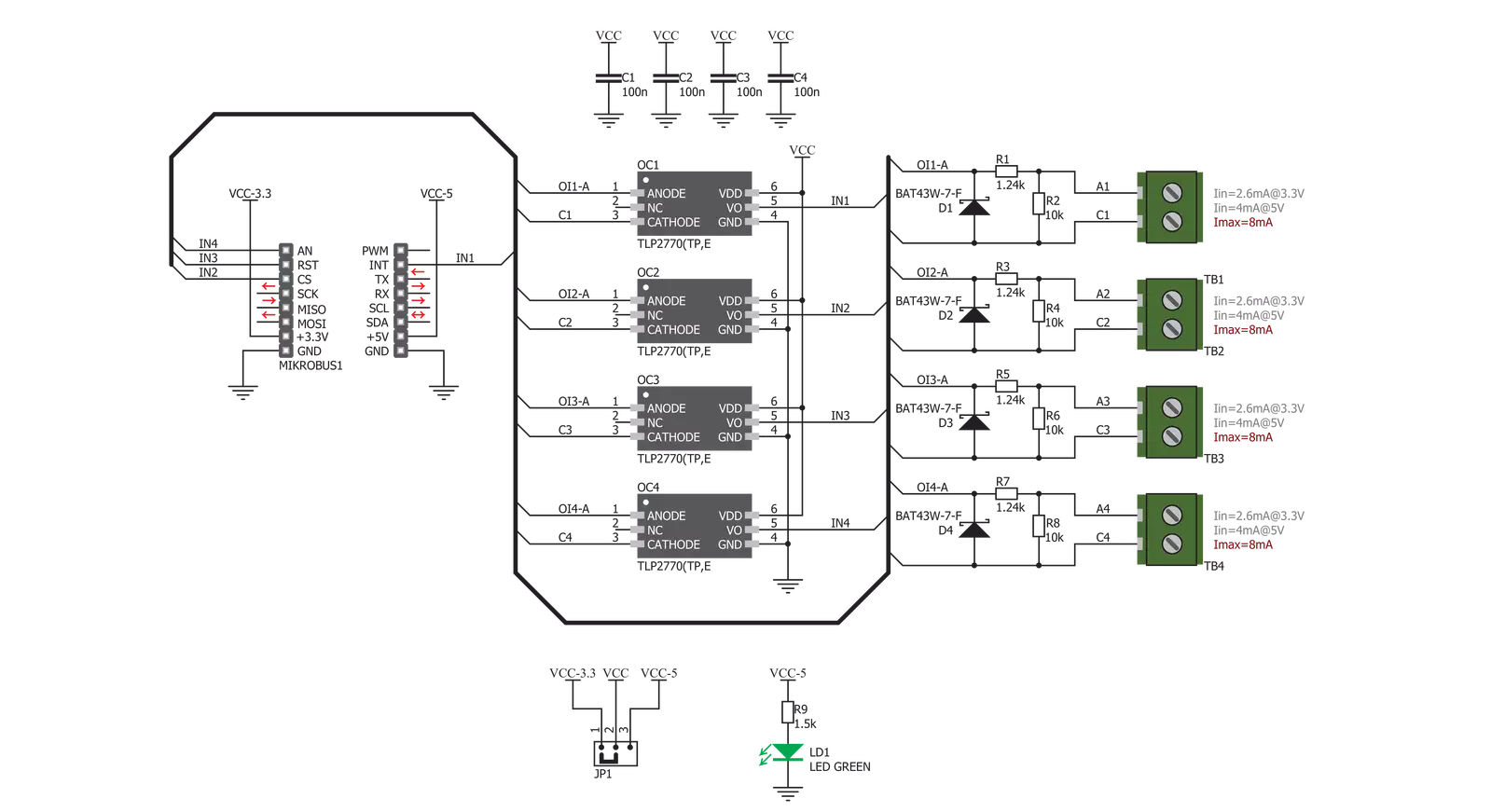
Opto 2 Click is based on four TLP2770, 20Mbps low-power optocouplers from Toshiba Semiconductor. These are fast optocouplers, with their output stages shielded against EMI, allowing them to work on higher speeds, providing common-mode transient immunity of ±20 kV/μs. The internal LED elements are driven with 4mA for 5V operation or 2.6mA for 3.3V operation. The input stages are also equipped with (Schottky) diodes, which prevents inverse polarization of the LED elements and thus, a permanent damage that might occur in that case. The working principle of the optocouplers is quite simple: A photo-emitting element - usually a LED, is encapsulated inside the die along with the photo-sensitive element, which can be a photo-sensitive transistor or a photo-diode. LEDs and photo-sensing elements are galvanically isolated, making the input and output electrical networks completely independent of each other. When the LED is biased, it emits light which in return causes the current to flow through
the photo-sensitive element. In these particular optocouplers, the output stage is additionally conditioned by a Schmitt trigger and it drives the output transistors which form a totem pole output stage. Having a totem pole output configuration allows the output stage to both sink and source current. The optocoupler inputs - the anodes (labeled as A) and cathodes (labeled as C) of the internal optocoupler LEDs, are routed to the screw terminals, which allow connection the external electrical circuit, used to trigger an event on the isolated MCU. The electrical potential between the anode and the cathode input of each optocoupler element should stay within the range between 3.3V and 5V. The optocoupler outputs are routed to the mikroBUS™ The mikroBUS™ pins INT, CS, RST, and AN, are routed to the optocoupler outputs 1, 2, 3, and 4, respectively, and are labeled as IN1, IN2, IN3, and IN4. As already mentioned, the output stages are conditioned with the Schmitt trigger circuit, reducing the input noise sensitivity
and false triggering. The Faraday shield protects the output stages against EMI and provides common-mode transient immunity of ±20 kV/μs. Although these mikroBUS™ pins are labeled as IN1 to IN4, they are actually outputs from the optocouplers, and it is highly recommended to use them as the INPUT pins on the host MCU. The Click board™ is equipped with an SMD jumper labeled as LOGIC, which allows selection of the voltage, applied to the optocoupler output stage. This voltage effectively determines the logic voltage level for the MCU pins. It can be selected between 3.3V and 5V, allowing this Click board™ to be interfaced with both 3.3V and 5V MCUs. The provided library offers functions that simplify and speed up the application development. The included example application demonstrates their use. This application can be used as a reference for custom projects.


Features overview
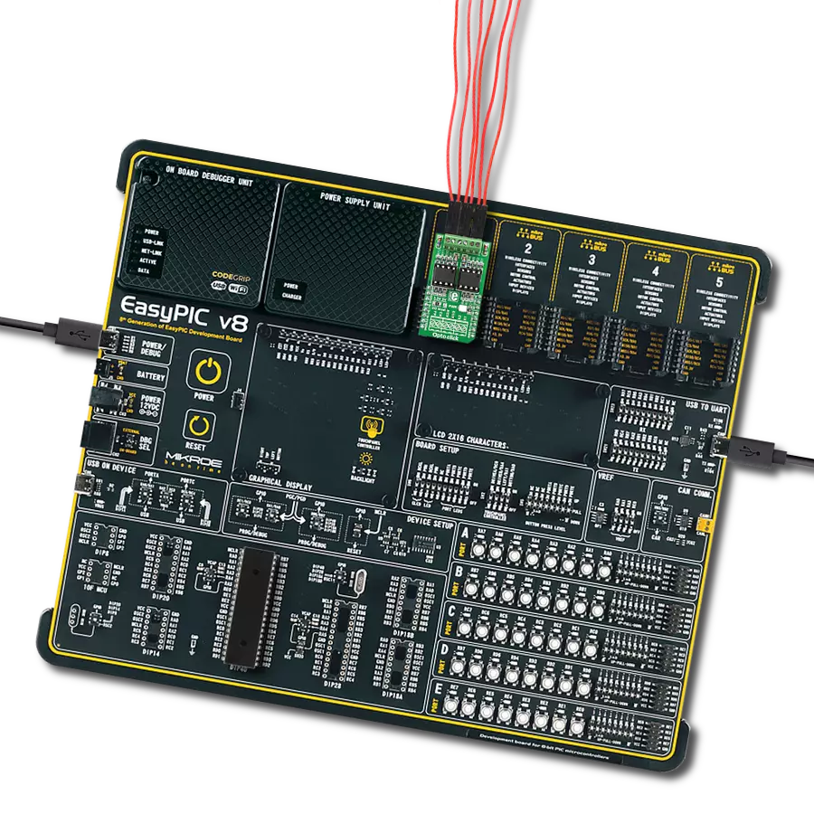
Development board
Curiosity PIC32 MZ EF development board is a fully integrated 32-bit development platform featuring the high-performance PIC32MZ EF Series (PIC32MZ2048EFM) that has a 2MB Flash, 512KB RAM, integrated FPU, Crypto accelerator, and excellent connectivity options. It includes an integrated programmer and debugger, requiring no additional hardware. Users can expand
functionality through MIKROE mikroBUS™ Click™ adapter boards, add Ethernet connectivity with the Microchip PHY daughter board, add WiFi connectivity capability using the Microchip expansions boards, and add audio input and output capability with Microchip audio daughter boards. These boards are fully integrated into PIC32’s powerful software framework, MPLAB Harmony,
which provides a flexible and modular interface to application development a rich set of inter-operable software stacks (TCP-IP, USB), and easy-to-use features. The Curiosity PIC32 MZ EF development board offers expansion capabilities making it an excellent choice for a rapid prototyping board in Connectivity, IOT, and general-purpose applications.

Microcontroller Overview
MCU Card / MCU
Architecture
PIC32
MCU Memory (KB)
2048
Silicon Vendor
Microchip
Pin count
100
RAM (Bytes)
524288
Used MCU Pins
mikroBUS™ mapper
Take a closer look
Click board™ Schematic
Step by step
Project assembly

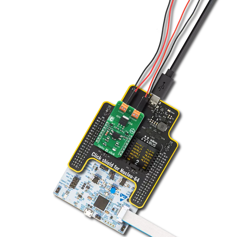
Start by selecting your development board and Click board™. Begin with the Curiosity PIC32 MZ EF as your development board.


Software Support
Library Description
This library contains API for Opto 2 Click driver.
Key functions:
opto2_check_out1- OUT1 Check functionopto2_check_out2- OUT2 Check functionopto2_check_out3- OUT3 Check function
Open Source
Code example
The complete application code and a ready-to-use project are available through the NECTO Studio Package Manager for direct installation in the NECTO Studio. The application code can also be found on the MIKROE GitHub account.
/*!
 * \file
 * \brief Opto 2 Click example
 *
 * # Description
 * This application used to provide an optical isolation of sensitive microcontroller.
 *
 * The demo application is composed of two sections :
 *
 * ## Application Init
 * Initializes device selects the outputs (OUT1 - OUT4) which state be checked.
 *
 * ## Application Task
 * Performs the check procedure for selected outputs and logs the states from that
  outputs on USB UART. Repeat the check procedure every 2 seconds.

 *
 * \author MikroE Team
 *
 */
// ------------------------------------------------------------------- INCLUDES

#include "board.h"
#include "log.h"
#include "opto2.h"

// ------------------------------------------------------------------ VARIABLES

static opto2_t opto2;
static log_t logger;

static uint8_t sel_output;

// ------------------------------------------------------ APPLICATION FUNCTIONS

void opto2_set_logger ( uint8_t sel_out1, uint8_t sel_out2, uint8_t sel_out3, uint8_t sel_out4 )
{

    if ( sel_out1 > 1 )
    {
        sel_out1 = 1;
    }
    if ( sel_out2 > 1 )
    {
        sel_out2 = 1;
    }
    if ( sel_out3 > 1 )
    {
        sel_out3 = 1;
    }
    if ( sel_out4 > 1 )
    {
        sel_out4 = 1;
    }

    sel_output = 0;
    sel_output |= sel_out1;
    sel_output |= sel_out2 << 1;
    sel_output |= sel_out3 << 2;
    sel_output |= sel_out4 << 3;
}

void application_init ( void )
{
    log_cfg_t log_cfg;
    opto2_cfg_t cfg;

    /**
     * Logger initialization.
     * Default baud rate: 115200
     * Default log level: LOG_LEVEL_DEBUG
     * @note If USB_UART_RX and USB_UART_TX
     * are defined as HAL_PIN_NC, you will
     * need to define them manually for log to work.
     * See @b LOG_MAP_USB_UART macro definition for detailed explanation.
     */
    LOG_MAP_USB_UART( log_cfg );
    log_init( &logger, &log_cfg );

    opto2_cfg_setup( &cfg );
    OPTO2_MAP_MIKROBUS( cfg, MIKROBUS_1 );
    opto2_init( &opto2, &cfg );

    log_info( &logger, "---- Application Init ----" );

    opto2_set_logger( 1, 1, 0, 0 );
    log_printf( &logger, "OPTO 2 is initialized \r\n" );
    log_printf( &logger, "" );
    Delay_ms ( 200 );
}

void application_task ( void )
{
    uint8_t check_output;
    uint8_t cnt;
    uint8_t tmp;

    tmp = 1;

    for ( cnt = 0; cnt < 4; cnt++ )
    {
        switch ( sel_output & tmp )
        {
            case 0x01 :
            {
                check_output = opto2_check_out1( &opto2 );

                if ( check_output == 0 )
                {
                    log_printf( &logger, "OUT1 is low\r\n" );
                }
                else
                {
                    log_printf( &logger, "OUT1 is high\r\n" );
                }
                break;
            }
            case 0x02 :
            {
                check_output = opto2_check_out2( &opto2 );

                if ( check_output == 0 )
                {
                    log_printf( &logger, "OUT2 is low\r\n" );
                }
                else
                {
                    log_printf( &logger, "OUT2 is high\r\n" );
                }
                break;
            }
            case 0x04 :
            {
                check_output = opto2_check_out3( &opto2 );

                if ( check_output == 0 )
                {
                    log_printf( &logger, "OUT3 is low\r\n" );
                }
                else
                {
                    log_printf( &logger, "OUT3 is high\r\n" );
                }
                break;
            }
            case 0x08 :
            {
                check_output = opto2_check_out4( &opto2 );

                if ( check_output == 0 )
                {
                    log_printf( &logger, "OUT4 is low\r\n" );
                }
                else
                {
                    log_printf( &logger, "OUT4 is high\r\n" );
                }
                break;
            }
            default :
            {
                break;
            }
        }

        tmp <<= 1;
    }

    Delay_ms ( 1000 );
    Delay_ms ( 1000 );
}

int main ( void )
{
    /* Do not remove this line or clock might not be set correctly. */
    #ifdef PREINIT_SUPPORTED
    preinit();
    #endif

    application_init( );

    for ( ; ; )
    {
        application_task( );
    }

    return 0;
}

// ------------------------------------------------------------------------ END
Additional Support
Resources
Category:Optocoupler