Improve system reliability with TLP241A and PIC18F2680 through robust electrical isolation
Elevate signal integrity: OptoLink isolation at Its best!
Published Nov 01, 2023
Click board™
Opto 3 Click
Dev. board
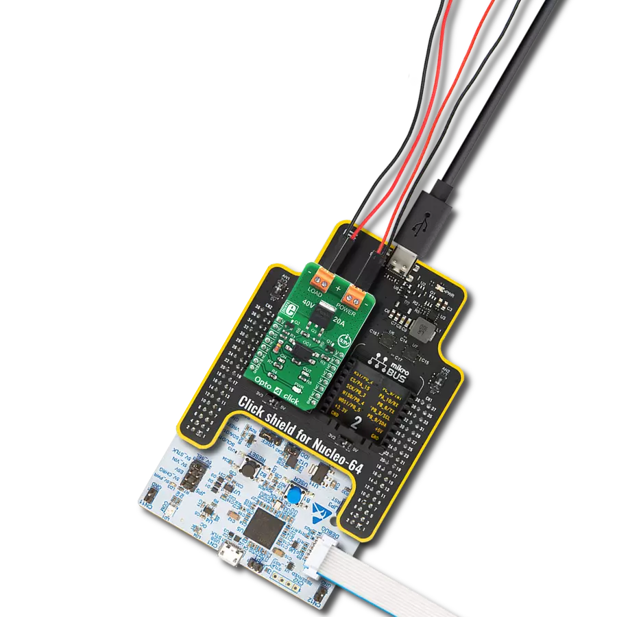
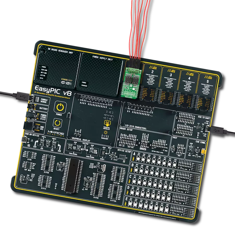
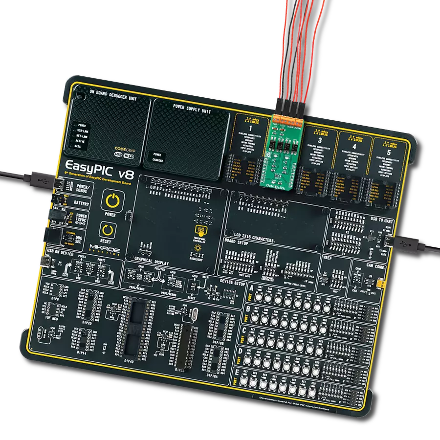
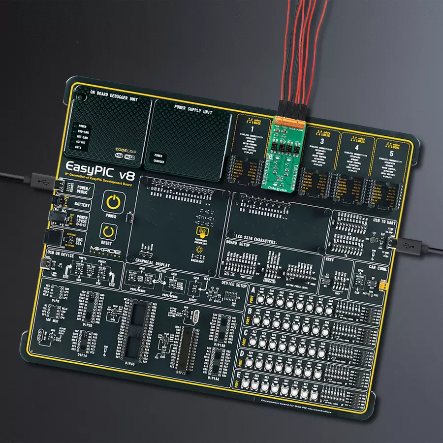
EasyPIC v8
Compiler
NECTO Studio
MCU
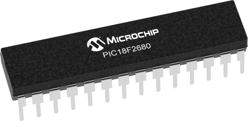
PIC18F2680
Provide complete electrical isolation, ensuring your sensitive signals remain unaffected by external interference.
A
A
Hardware Overview
How does it work?
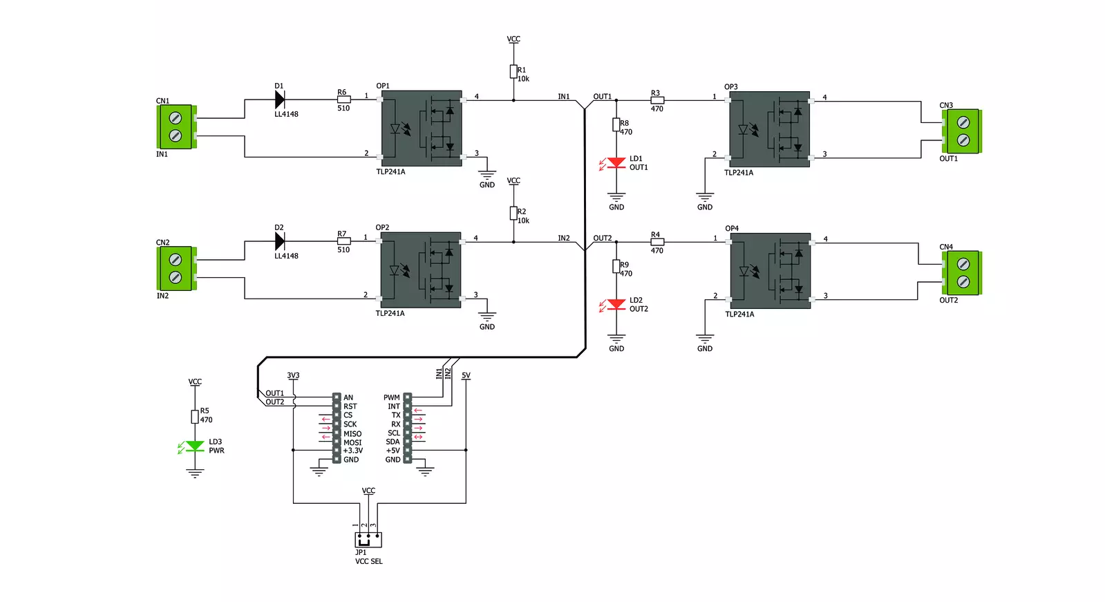
Opto 3 Click is based on two pairs of normally opened, high-quality solid-state relays labeled as TLP241A, from Toshiba Semiconductor. The TLP241A is an optically isolated solid-state relay (SSR), featuring an integrated IR LED and two output MOSFETs. The output stage does not have any electrical contact with the input stage; it is activated by infrared light, produced by an integrated IR LED. This allows reinforced galvanic isolation between the input and the output stage. The output stage can sustain up to 40V while OFF. When activated, due to a very low RDSON of the integrated MOSFETs, it can conduct up to 2A of current. The TLP241A are able to effectively replace traditionally used mechanical relays, bringing up the full set of inherited benefits: virtually unlimited number of cycles since there are no moving parts that would wear off, no bouncing effect on the output contacts, high resistance to mechanical shock and environmental influence, low current required for the activation, constant resistance since no carbon and rust can build up on contacts, there is no sparking or electric arc forming while operated, compact size, higher isolation voltage, and so on. However, unlike optocouplers (similar devices which are designed for much lower currents and voltages), SSRs are not designed
to be used as signal line isolators. SSR typically has a slow signal propagation time. Still, it can be used for various communication protocols which use lower data rates, including UART/RS232, 1-Wire, and similar. One pair of SSRs is driven by the host MCU. This pair can be used to activate an external circuit, utilizing the full potential of the TLP241A SSR. One or two SSRs can be used as relays, allowing the host MCU to control heavier loads such as DC motors, some other electrical circuit which operates on higher potential, LED strips, LED arrays, and more. A HIGH logic level on mikroBUS™ pins AN or RST labeled as OU1 and OU2 respectively, will activate the integrated IR LED. It will turn ON the MOSFETs in the SSR, allowing the current to flow through an external circuit. Two red LEDs, labeled as OUT1 and OUT 2, are connected to each of the MCU output pins. These LEDs provide visual feedback about the SSR state: if ON, the respective SSR is in a conductive state. SSR outputs are routed to two screw terminals labeled as OUT1 and OUT2, allowing an external circuit to be securely connected. The other pair of SSRs is used to provide optical isolation for external signals, offering protection for sensitive MCU pins that way. While the SSR is not activated, PWM and INT pins of the mikroBUS™
labeled as IN1 and IN2 respectively, are pulled to a HIGH logic level by a resistor. A signal on the input terminal will activate the respective SSR, pulling the IN1 (IN2) pin to a LOW logic level. Since galvanically isolated, the signal at the input terminal can be at a different potential than the host MCU, preventing any stray currents to flow between two GNDs. This will also protect the host MCU from the electrostatic discharge (ESD) that might occur. It is important to connect the input signal correctly. Therefore, two input terminals have their ports clearly labeled with + and - signs. A Schottky diode in series provides some protection to the input IR LED, however, care should be taken not to exceed specifications from the TLP241A datasheet. Pull-up resistors on the input side SSRs are connected to the power supply from mikroBUS™, providing a HIGH logic level while the SSR is not active. The voltage of the power supply directly determines the voltage level that will be applied to IN1 and IN2 pins in this case. Therefore, an SMD jumper labeled as VCC SEL is provided on the Click board™, allowing the user to select the logic voltage level between 3.3V and 5V, depending on the used MCU and its capabilities.


Features overview
Development board
EasyPIC v8 is a development board specially designed for the needs of rapid development of embedded applications. It supports many high pin count 8-bit PIC microcontrollers from Microchip, regardless of their number of pins, and a broad set of unique functions, such as the first-ever embedded debugger/programmer. The development board is well organized and designed so that the end-user has all the necessary elements, such as switches, buttons, indicators, connectors, and others, in one place. Thanks to innovative manufacturing technology, EasyPIC v8 provides a fluid and immersive working experience, allowing access anywhere and under any
circumstances at any time. Each part of the EasyPIC v8 development board contains the components necessary for the most efficient operation of the same board. In addition to the advanced integrated CODEGRIP programmer/debugger module, which offers many valuable programming/debugging options and seamless integration with the Mikroe software environment, the board also includes a clean and regulated power supply module for the development board. It can use a wide range of external power sources, including a battery, an external 12V power supply, and a power source via the USB Type-C (USB-C) connector.
Communication options such as USB-UART, USB DEVICE, and CAN are also included, including the well-established mikroBUS™ standard, two display options (graphical and character-based LCD), and several different DIP sockets. These sockets cover a wide range of 8-bit PIC MCUs, from the smallest PIC MCU devices with only eight up to forty pins. EasyPIC v8 is an integral part of the Mikroe ecosystem for rapid development. Natively supported by Mikroe software tools, it covers many aspects of prototyping and development thanks to a considerable number of different Click boards™ (over a thousand boards), the number of which is growing every day.

Microcontroller Overview
MCU Card / MCU
Architecture
PIC
MCU Memory (KB)
64
Silicon Vendor
Microchip
Pin count
28
RAM (Bytes)
3328
Used MCU Pins
mikroBUS™ mapper
Take a closer look
Click board™ Schematic
Step by step
Project assembly

Start by selecting your development board and Click board™. Begin with the EasyPIC v8 as your development board.


Software Support
Library Description
This library contains API for Opto 3 Click driver.
Key functions:
opto3_get_in1- This function gets input 1 pin stateopto3_get_in2- This function gets input 2 pin stateopto3_set_out1- This function sets output 1 pin state.
Open Source
Code example
The complete application code and a ready-to-use project are available through the NECTO Studio Package Manager for direct installation in the NECTO Studio. The application code can also be found on the MIKROE GitHub account.
/*!
 * \file
 * \brief Opto 3 Click example
 *
 * # Description
 * Opto 3 Click to be used in applications that require reinforced galvanic
 * isolation for both their input and output stages.
 *
 * The demo application is composed of two sections :
 *
 * ## Application Init
 * Initializes GPIO interface.
 *
 * ## Application Task
 * Reads the input pins state and sets their respective output pins to the same logic state.
 * The output pins state will be displayed on the USB UART where you can track their changes.
 *
 * \author MikroE Team
 *
 */
// ------------------------------------------------------------------- INCLUDES

#include "board.h"
#include "log.h"
#include "opto3.h"

// ------------------------------------------------------------------ VARIABLES

static opto3_t opto3;
static log_t logger;

// ------------------------------------------------------ APPLICATION FUNCTIONS

void application_init ( void )
{
    log_cfg_t log_cfg;
    opto3_cfg_t cfg;

    /**
     * Logger initialization.
     * Default baud rate: 115200
     * Default log level: LOG_LEVEL_DEBUG
     * @note If USB_UART_RX and USB_UART_TX
     * are defined as HAL_PIN_NC, you will
     * need to define them manually for log to work.
     * See @b LOG_MAP_USB_UART macro definition for detailed explanation.
     */
    LOG_MAP_USB_UART( log_cfg );
    log_init( &logger, &log_cfg );
    log_info( &logger, " Application Init " );

    // Click initialization.
    opto3_cfg_setup( &cfg );
    OPTO3_MAP_MIKROBUS( cfg, MIKROBUS_1 );
    opto3_init( &opto3, &cfg );

    log_info( &logger, " Application Task " );
}

void application_task ( void )
{
    static uint8_t out1_state = 0;
    static uint8_t out2_state = 0;
    uint8_t in1_state = 0;
    uint8_t in2_state = 0;

    in1_state = opto3_get_in1( &opto3 );
    in2_state = opto3_get_in2( &opto3 );

    if ( in1_state != out1_state )
    {
        out1_state = in1_state;
        opto3_set_out1( &opto3, out1_state );
        log_printf( &logger, " OUT1 state: %u\r\n", ( uint16_t ) out1_state );
    }

    if ( in2_state != out2_state )
    {
        out2_state = in2_state;
        opto3_set_out2( &opto3, out2_state );
        log_printf( &logger, " OUT2 state: %u\r\n", ( uint16_t ) out2_state );
    }
}

int main ( void )
{
    /* Do not remove this line or clock might not be set correctly. */
    #ifdef PREINIT_SUPPORTED
    preinit();
    #endif

    application_init( );

    for ( ; ; )
    {
        application_task( );
    }

    return 0;
}


// ------------------------------------------------------------------------ END