Encode analog signal into a binary code easily with ADS7828 and PIC18F27K42
Convert with clarity
Published Dec 29, 2023
Click board™
ADC 12 Click
Dev. board
EasyPIC v7
Compiler
NECTO Studio
MCU
PIC18F27K42
Ready to take on even the most complex designs? Our ADC is up to the challenge!
A
A
Hardware Overview
How does it work?
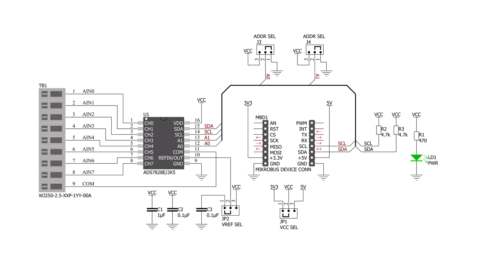
ADC 12 Click is based on the ADS7828, a low-power 12-bit data acquisition device with a serial I2C interface and an 8-channel multiplexer from Texas Instruments. The architecture of the ADS7828, which is a classic Successive Approximation Register (SAR) A/D converter, is based on capacitive redistribution that inherently includes a sample-and-hold function. It has an integrated I2C input and output port with screw terminal connectors for each analog input channel. An internally generated free-running clock controls it. When the ADS7828 is not performing conversions or being addressed, it keeps the A/D converter core powered off, and the internal clock does not operate. When the A/D converter enters the Hold mode, the voltage on the selected channel pin of the input
terminal is captured on the internal capacitor array. The input current on the analog inputs depends on the conversion rate of the device. During the sample period, the source must charge the internal sampling capacitor. There is no further input current after the capacitor has been fully charged. The amount of charge transfer from the analog source to the converter is a function of the conversion rate. ADC 12 Click communicates with MCU using the standard I2C 2-Wire interface with a frequency of up to 100kHz in the Standard, up to 400kHz in the Fast, and up to 3.4MHz in the High-Speed mode. It also allows the choice of the last two least significant bits (LSB), A0 and A1, by positioning SMD jumpers labeled ADDR SEL to an appropriate position marked as 0 and 1.
This Click board™ also possesses a jumper for selecting the reference voltage labeled as VREF SEL. The ADS7828 can operate with an internal 2.5V reference or an external reference (in this case, logic voltage level VCC), which can be selected by positioning SMD jumpers to an appropriate position marked as INT and EXT. This Click board™ can operate with either 3.3V or 5V logic voltage levels selected via the VCC SEL jumper. This way, both 3.3V and 5V capable MCUs can use the communication lines properly. However, the Click board™ comes equipped with a library containing easy-to-use functions and an example code that can be used, as a reference, for further development.


Features overview
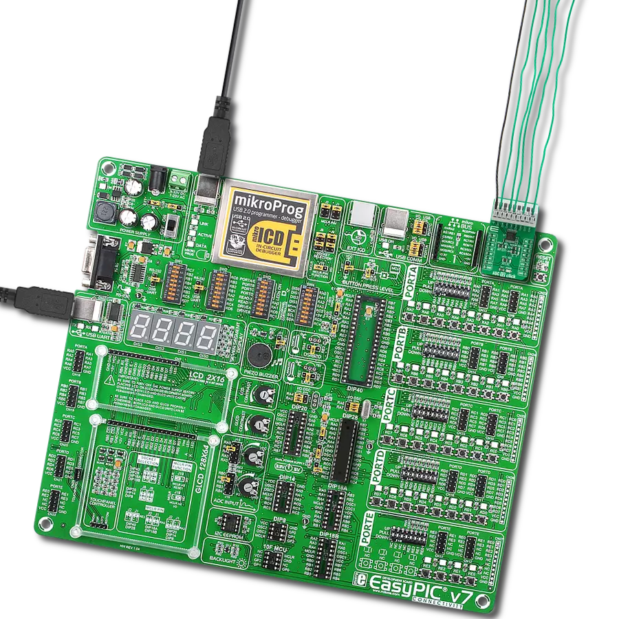
Development board
EasyPIC v7 is the seventh generation of PIC development boards specially designed to develop embedded applications rapidly. It supports a wide range of 8-bit PIC microcontrollers from Microchip and has a broad set of unique functions, such as a powerful onboard mikroProg programmer and In-Circuit debugger over USB-B. The development board is well organized and designed so that the end-user has all the necessary elements in one place, such as switches, buttons, indicators, connectors, and others. With four different connectors for each port, EasyPIC v7 allows you to connect accessory boards, sensors, and custom electronics more efficiently than ever. Each part of
the EasyPIC v7 development board contains the components necessary for the most efficient operation of the same board. An integrated mikroProg, a fast USB 2.0 programmer with mikroICD hardware In-Circuit Debugger, offers many valuable programming/debugging options and seamless integration with the Mikroe software environment. Besides it also includes a clean and regulated power supply block for the development board. It can use various external power sources, including an external 12V power supply, 7-23V AC or 9-32V DC via DC connector/screw terminals, and a power source via the USB Type-B (USB-B) connector. Communication options such as
USB-UART and RS-232 are also included, alongside the well-established mikroBUS™ standard, three display options (7-segment, graphical, and character-based LCD), and several different DIP sockets. These sockets cover a wide range of 8-bit PIC MCUs, from PIC10F, PIC12F, PIC16F, PIC16Enh, PIC18F, PIC18FJ, and PIC18FK families. EasyPIC v7 is an integral part of the Mikroe ecosystem for rapid development. Natively supported by Mikroe software tools, it covers many aspects of prototyping and development thanks to a considerable number of different Click boards™ (over a thousand boards), the number of which is growing every day.

Microcontroller Overview
MCU Card / MCU
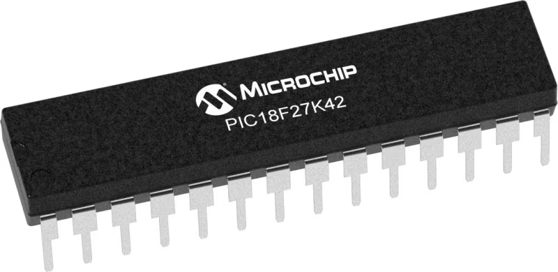
Architecture
PIC
MCU Memory (KB)
128
Silicon Vendor
Microchip
Pin count
28
RAM (Bytes)
8192
Used MCU Pins
mikroBUS™ mapper
Take a closer look
Click board™ Schematic
Step by step
Project assembly

Start by selecting your development board and Click board™. Begin with the EasyPIC v7 as your development board.


Software Support
Library Description
This library contains API for ADC 12 Click driver.
Key functions:
void adc12_send_cmd ( uint8_t cmd_byte );- Function is used to configure the device.uint16_t adc12_single_ended ( uint8_t chan, uint16_t v_ref );- Function is used to get raw ADC value.uint16_t adc12_differential ( uint8_t chan, uint16_t v_ref );- Function is used to get raw ADC value.
Open Source
Code example
The complete application code and a ready-to-use project are available through the NECTO Studio Package Manager for direct installation in the NECTO Studio. The application code can also be found on the MIKROE GitHub account.
/*!
 * @file main.c
 * @brief ADC12 Click example
 *
 * # Description
 * This example demonstrates the use of ADC 12 Click board.
 *
 * The demo application is composed of two sections :
 *
 * ## Application Init
 * Initializes the driver and sets the input and power-down modes.
 *
 * ## Application Task
 * Reads the RAW ADC data and converts it to voltage in milivolts and displays
 * both values on the USB UART every second.
 *
 * @note
 * With internal reference voltage set the Click measures up to 2500 mV.
 *
 * @author Stefan Filipovic
 *
 */

#include "board.h"
#include "log.h"
#include "adc12.h"

static adc12_t adc12;
static log_t logger;

void application_init ( void )
{
    log_cfg_t log_cfg;  /**< Logger config object. */
    adc12_cfg_t adc12_cfg;  /**< Click config object. */

    /**
     * Logger initialization.
     * Default baud rate: 115200
     * Default log level: LOG_LEVEL_DEBUG
     * @note If USB_UART_RX and USB_UART_TX
     * are defined as HAL_PIN_NC, you will
     * need to define them manually for log to work.
     * See @b LOG_MAP_USB_UART macro definition for detailed explanation.
     */
    LOG_MAP_USB_UART( log_cfg );
    log_init( &logger, &log_cfg );
    log_info( &logger, " Application Init " );

    // Click initialization.

    adc12_cfg_setup( &adc12_cfg );
    ADC12_MAP_MIKROBUS( adc12_cfg, MIKROBUS_1 );
    err_t init_flag = adc12_init( &adc12, &adc12_cfg );
    if ( init_flag == I2C_MASTER_ERROR )
    {
        log_error( &logger, " Application Init Error. " );
        log_info( &logger, " Please, run program again... " );

        for ( ; ; );
    }

    adc12_set_sd_mode ( &adc12, ADC12_CMD_SD_SINGLE_END );
    adc12_set_pd_mode( &adc12, ADC12_CMD_PD_IRON_ADON );
    log_info( &logger, " Application Task " );
}

void application_task ( void )
{
    uint16_t raw_adc;
    float voltage;

    adc12_read_raw_data ( &adc12, ADC12_SINGLE_END_CH0, &raw_adc );
    adc12_read_voltage ( &adc12, ADC12_SINGLE_END_CH0, ADC12_INTERNAL_VREF, &voltage );

    log_printf( &logger, " RAW ADC: %u \r\n", raw_adc );
    log_printf( &logger, " Voltage from Channel 0: %.2f mV \r\n", voltage );
    log_printf( &logger, " ---------------------------\r\n" );
    Delay_ms ( 1000 );
}

int main ( void )
{
    /* Do not remove this line or clock might not be set correctly. */
    #ifdef PREINIT_SUPPORTED
    preinit();
    #endif

    application_init( );

    for ( ; ; )
    {
        application_task( );
    }

    return 0;
}

// ------------------------------------------------------------------------ END


