Experience ultra-responsive pulse generation with LTC6993-2 and STM32F407VGT6
“One-shot” pulse generator

Published Dec 29, 2023
Click board™
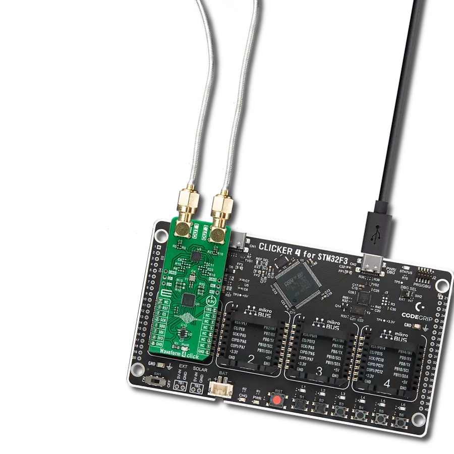
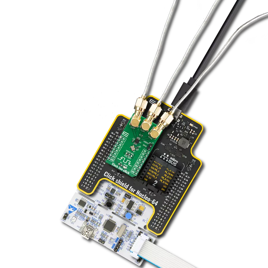
One Shot Click
Dev. board
Clicker 4 for STM32F4
Compiler
NECTO Studio
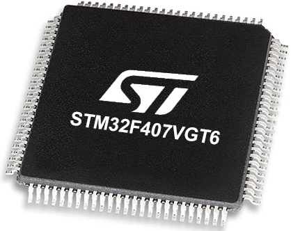
MCU
STM32F407VGT6
Create accurately timed pulses, and ensure synchronized operations in various systems and devices
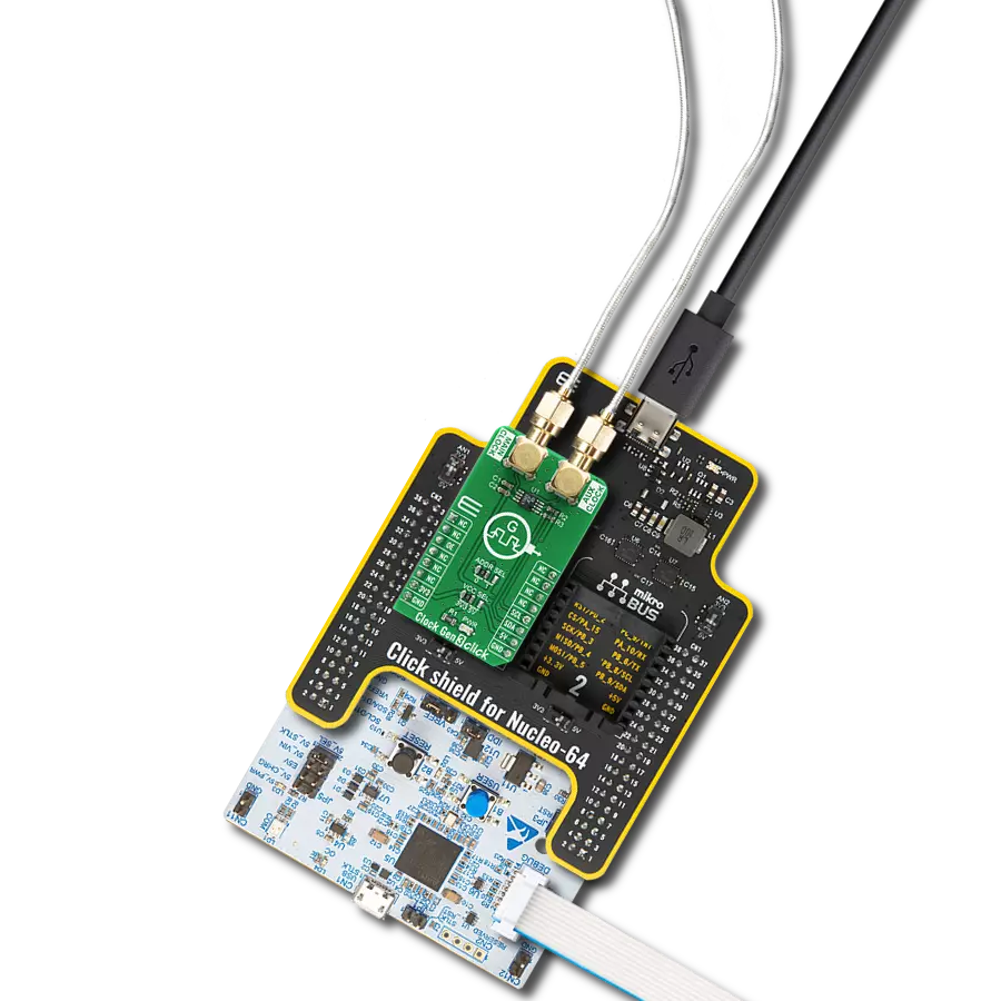
A
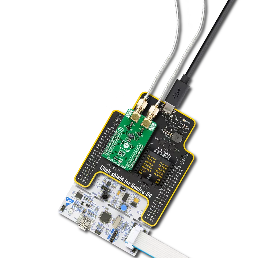
A
Hardware Overview
How does it work?
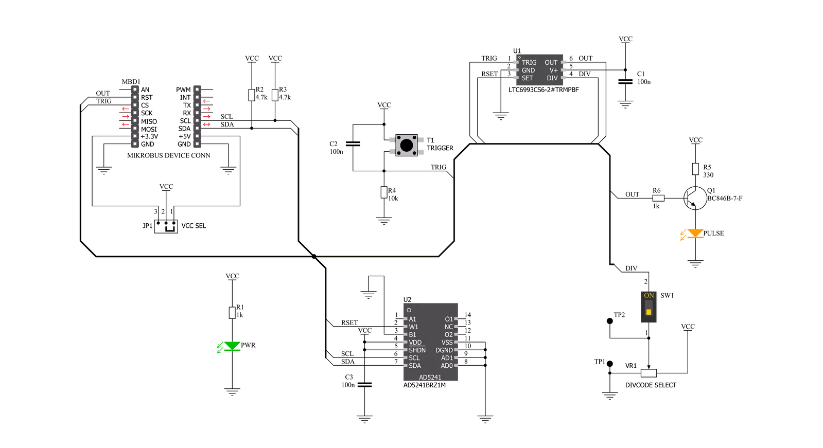
One Shot Click is based on the LTC6993-2, a monostable multivibrator (also known as a "one-shot" pulse generator) with a programmable pulse width of 1μs to 33.6 seconds from Analog Devices. The LTC6993-2 is part of the TimerBlox® family of versatile silicon timing devices. A single resistor, RSET, programs an internal master oscillator frequency, setting the LTC6993's time base. The output pulse width is determined by this master oscillator and an internal clock divider, NDIV, programmable to eight settings from 1 to 221. The output pulse is initiated by a transition on the trigger input (TRIG). Each part can be configured to generate positive or negative output pulses. The LTC6993-2 has four versions to provide different trigger signal polarity and retrigger capability. Besides that, LTC6993-2 also offers the ability to dynamically adjust the width of the output pulse via a separate control voltage brought to the SET
pin of the IC. A simple trimmer or potentiometer could be used; however, due to reliability reasons, the AD5241 digital potentiometer is used for that purpose on One Shot Click. The word is also about a 256-position digital potentiometer with a low-temperature coefficient (30 ppm/°C) from Analog Devices. The AD5241 communicates with the microcontroller over the standard I2C interface so that the user can easily control and precisely calculate the output pulse width just by simply setting the wiper value in the AD5241 registers. One Shot Click also contains the multi-turn trimmer wired as a resistor divider between V+ and GND and brought to the DIV pin of the LTC6993-2. The DIV pin is the programmable divider and polarity input. The polarity input, which pin voltage is internally converted into a 4-bit result (DIVCODE). The MSB of DIVCODE (POL) determines the polarity of the OUT pins. When
POL = 0, the output produces a positive pulse. When POL = 1, the output produces a negative pulse. That way, the user can easily set the output pulse width range, and polarity by setting the desired voltage on the trimmer mentioned (VR1). This Click also contains test points to ease the user's access to the referent voltage. One can separate the trimmer from the rest of the circuit using the separation switch (SW1), then precisely set and measure the desired voltage and turn the switch back in the ON position. This Click board™ can operate with either 3.3V or 5V logic voltage levels selected via the VCC SEL jumper. This way, both 3.3V and 5V capable MCUs can use the communication lines properly. Also, this Click board™ comes equipped with a library containing easy-to-use functions and an example code that can be used, as a reference, for further development.

Features overview
Development board
Clicker 4 for STM32F4 is a compact development board designed as a complete solution that you can use to quickly build your own gadgets with unique functionalities. Featuring an STM32F407VGT6 MCU, four mikroBUS™ sockets for Click boards™ connectivity, power management, and more, it represents a perfect solution for the rapid development of many different types of applications. At its core is an STM32F407VGT6 MCU, a powerful microcontroller by STMicroelectronics based on the high-performance
Arm® Cortex®-M4 32-bit processor core operating at up to 168 MHz frequency. It provides sufficient processing power for the most demanding tasks, allowing Clicker 4 to adapt to any specific application requirements. Besides two 1x20 pin headers, four improved mikroBUS™ sockets represent the most distinctive connectivity feature, allowing access to a huge base of Click boards™, growing on a daily basis. Each section of Clicker 4 is clearly marked, offering an intuitive and clean interface. This makes working with the
development board much simpler and, thus, faster. The usability of Clicker 4 doesn’t end with its ability to accelerate the prototyping and application development stages: it is designed as a complete solution that can be implemented directly into any project, with no additional hardware modifications required. Four mounting holes [4.2mm/0.165”] at all four corners allow simple installation by using mounting screws.

Microcontroller Overview
MCU Card / MCU
Architecture
ARM Cortex-M4
MCU Memory (KB)
10
Silicon Vendor
STMicroelectronics
Pin count
100
RAM (Bytes)
100
Used MCU Pins
mikroBUS™ mapper
Take a closer look
Click board™ Schematic
Step by step
Project assembly

Start by selecting your development board and Click board™. Begin with the Clicker 4 for STM32F4 as your development board.


Track your results in real time
Application Output
1. Application Output - In Debug mode, the 'Application Output' window enables real-time data monitoring, offering direct insight into execution results. Ensure proper data display by configuring the environment correctly using the provided tutorial.

2. UART Terminal - Use the UART Terminal to monitor data transmission via a USB to UART converter, allowing direct communication between the Click board™ and your development system. Configure the baud rate and other serial settings according to your project's requirements to ensure proper functionality. For step-by-step setup instructions, refer to the provided tutorial.

3. Plot Output - The Plot feature offers a powerful way to visualize real-time sensor data, enabling trend analysis, debugging, and comparison of multiple data points. To set it up correctly, follow the provided tutorial, which includes a step-by-step example of using the Plot feature to display Click board™ readings. To use the Plot feature in your code, use the function: plot(*insert_graph_name*, variable_name);. This is a general format, and it is up to the user to replace 'insert_graph_name' with the actual graph name and 'variable_name' with the parameter to be displayed.

Software Support
Library Description
This library contains API for One Shot Click driver.
Key functions:
oneshot_get_resistance- This function reads the resistance data from the AD5241 chiponeshot_digital_read_rst- This function reads the digital signal from the RST pinoneshot_digital_write_cs- This function writes the specified digital signal to the CS pin
Open Source
Code example
The complete application code and a ready-to-use project are available through the NECTO Studio Package Manager for direct installation in the NECTO Studio. The application code can also be found on the MIKROE GitHub account.
/*!
 * \file
 * \brief OneShot Click example
 *
 * # Description
 * This example shows the user how to configure and use the One Shot Click. The Click has a
 * monostable monovibrator which cam generate a pulse of width between 1μs and 33.6 seconds.
 *
 * The demo application is composed of two sections :
 *
 * ## Application Init
 * This function initializes and configures the logger and Click modules. Resistance data,
 * acquired from the AD5241, is displayed at the end of the initialization process.
 *
 * ## Application Task
 * This function triggers one shot every 8 seconds.
 *
 * \author MikroE Team
 *
 */
// ------------------------------------------------------------------- INCLUDES

#include "board.h"
#include "log.h"
#include "oneshot.h"

// ------------------------------------------------------------------ VARIABLES

static oneshot_t oneshot;
static log_t logger;

// ------------------------------------------------------ APPLICATION FUNCTIONS

void application_init ( )
{
    log_cfg_t log_cfg;
    oneshot_cfg_t cfg;

    /**
     * Logger initialization.
     * Default baud rate: 115200
     * Default log level: LOG_LEVEL_DEBUG
     * @note If USB_UART_RX and USB_UART_TX
     * are defined as HAL_PIN_NC, you will
     * need to define them manually for log to work.
     * See @b LOG_MAP_USB_UART macro definition for detailed explanation.
     */
    LOG_MAP_USB_UART( log_cfg );
    log_init( &logger, &log_cfg );
    log_info( &logger, "---- Application Init ----" );

    //  Click initialization.

    oneshot_cfg_setup( &cfg );
    ONESHOT_MAP_MIKROBUS( cfg, MIKROBUS_1 );
    oneshot_init( &oneshot, &cfg );
    Delay_100ms( );
    oneshot_default_cfg( &oneshot );
    Delay_100ms( );
    log_printf( &logger, " * Resistance: %.1f Ohm\r\n", oneshot_get_resistance( &oneshot ) );
}

void application_task ( )
{
    oneshot_digital_write_cs( &oneshot, 1 );
    Delay_ms ( 1 );
    oneshot_digital_write_cs( &oneshot, 0 );
    log_printf( &logger, " * One shot triggered \r\n" );
    log_printf( &logger, " --------------------------- \r\n" );
    // 8 seconds delay
    Delay_ms ( 1000 );
    Delay_ms ( 1000 );
    Delay_ms ( 1000 );
    Delay_ms ( 1000 );
    Delay_ms ( 1000 );
    Delay_ms ( 1000 );
    Delay_ms ( 1000 );
    Delay_ms ( 1000 );
}

int main ( void )
{
    /* Do not remove this line or clock might not be set correctly. */
    #ifdef PREINIT_SUPPORTED
    preinit();
    #endif

    application_init( );

    for ( ; ; )
    {
        application_task( );
    }

    return 0;
}

// ------------------------------------------------------------------------ END
Additional Support
Resources
Category:Clock generator