Create accurate square-wave pulses with LTC6904 and PIC18F25K80 for limitless possibilities
Timing perfected
Published May 27, 2023
Click board™
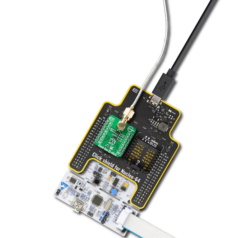
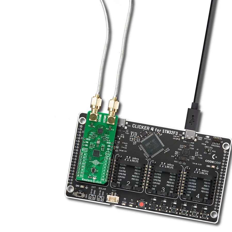
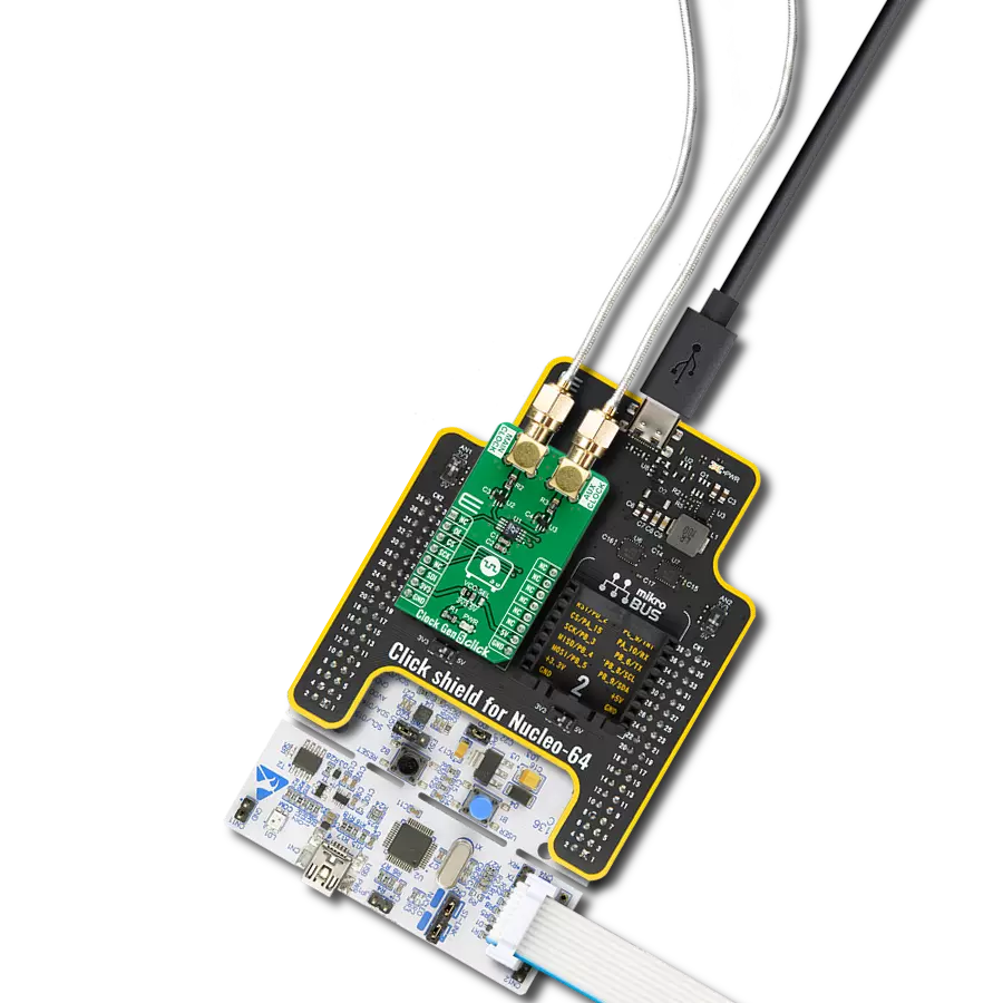
Clock Gen 3 Click
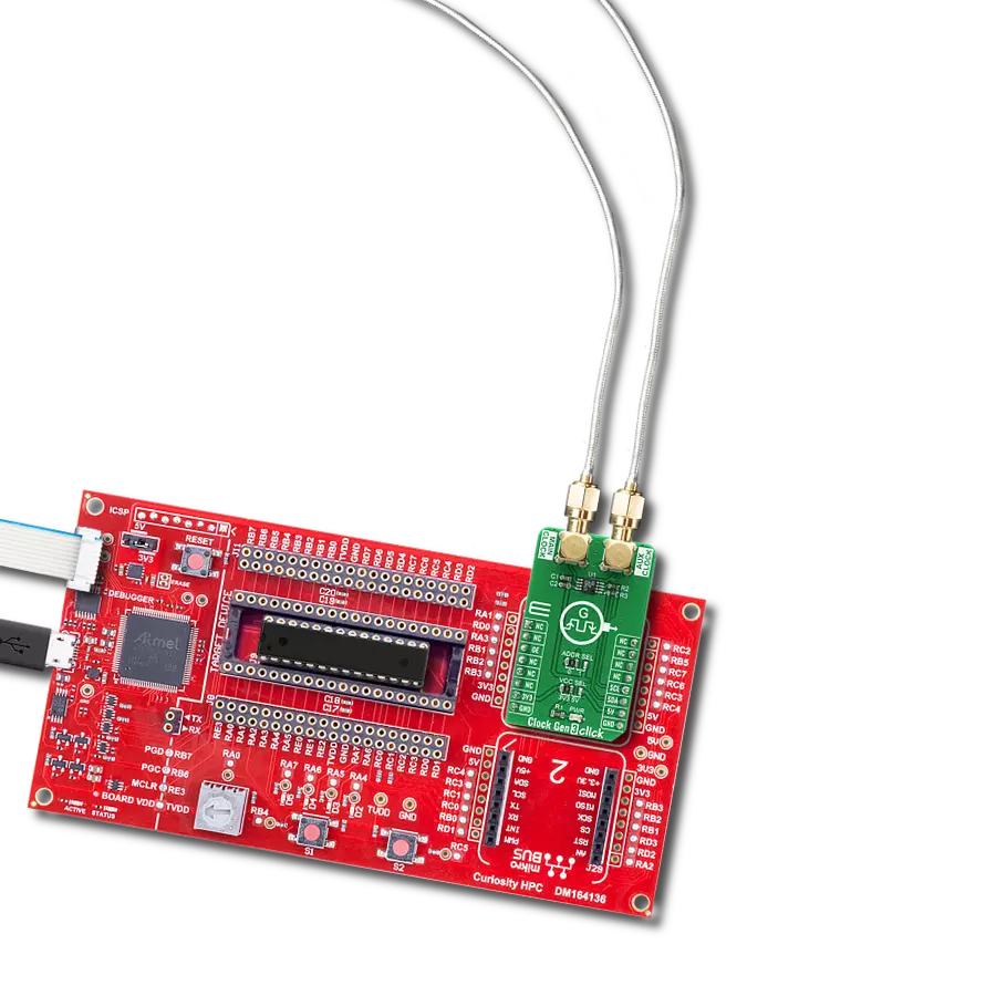
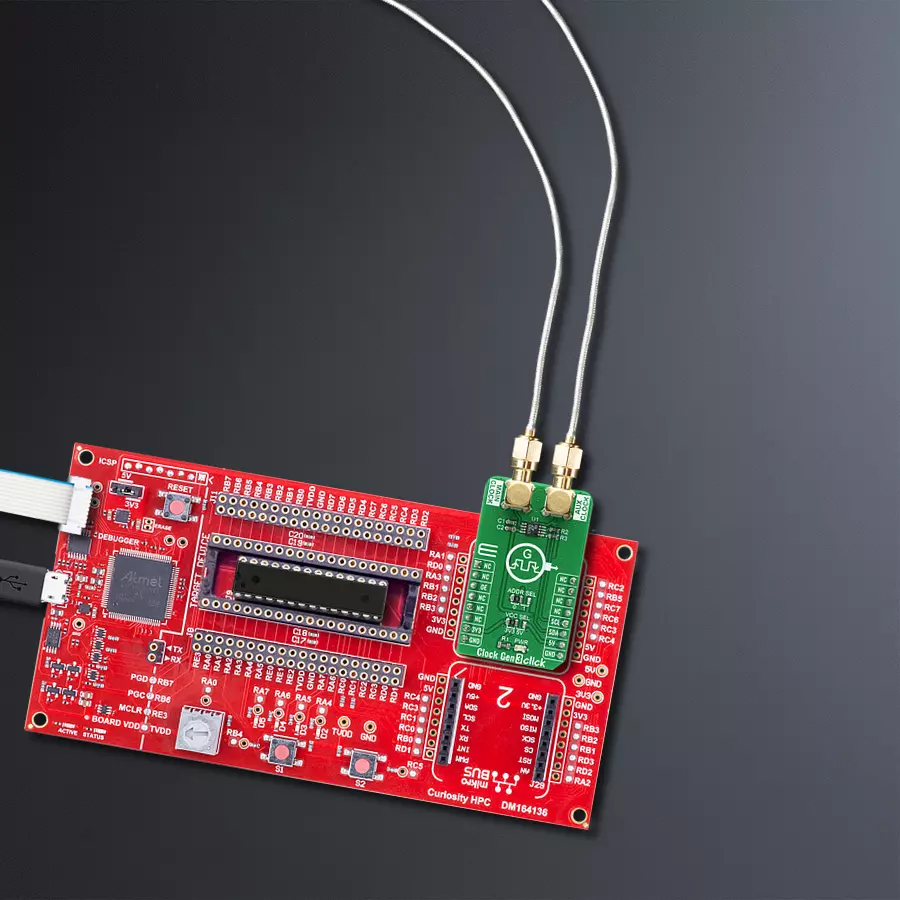
Dev. board
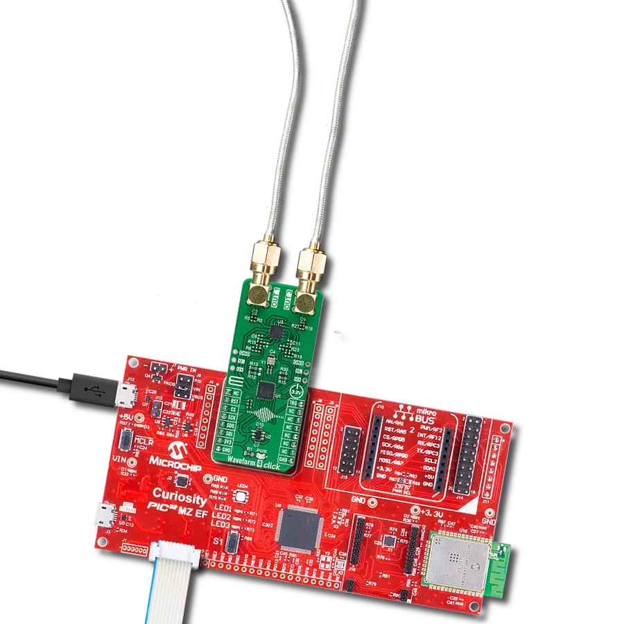
Curiosity HPC
Compiler
NECTO Studio
MCU
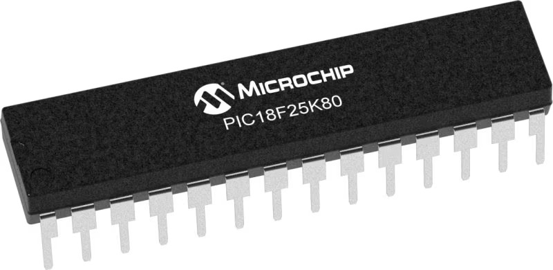
PIC18F25K80
Unlock seamless synchronization and precise timing in your engineering projects with a powerful clock generator
A
A
Hardware Overview
How does it work?
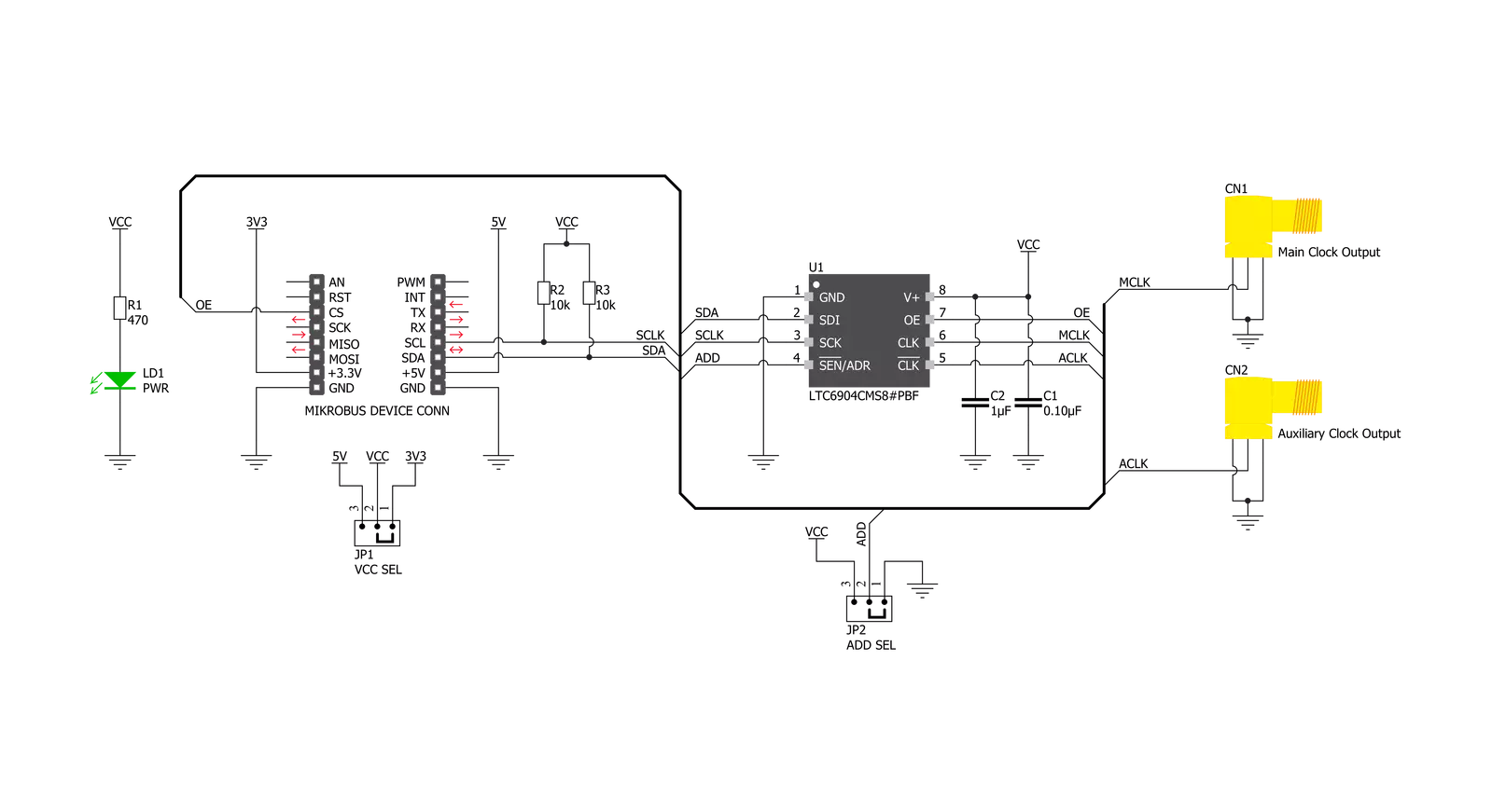
Clock Gen 3 Click is based on the LTC6904 IC, 1kHz to 68MHz Serial Port Programmable Oscillator from Linear Technology. The LTC6904 is a low-power self-contained digital frequency source providing a precision frequency from 1KHz to 68MHz, set by the I2C interface operating up to 3.4 Mbps. This Click board™ features onboard I2C address jumpers, pull-up resistors, a power supply bypass capacitor, and a power LED. The maximum frequency error is 1.1% or 1.6% when operating with a flexible power supply voltage range from 2.7V to 5V, which makes it suitable for 3.3V and 5V MCUs. In most frequency ranges, the output of the Clock Gen 3 Click is generated as a division of the higher internal clock frequency. This helps to minimize jitter and subharmonics at the output of the device.
In the highest frequency ranges, the division ratio is reduced, which will result in a greater cycle-to-cycle jitter as well as spurs at the internal sampling frequency. Because the internal control loop runs at 1MHz to 2MHz without regard to the output frequency, output spurs separated from the set frequency by 1MHz to 2MHz may be observed. These spurs are characteristically more than 30dB below the level of the set frequency. The LTC6904 communicates with the MCU using the standard I2C 2-wire interface. The two bus lines, SDA and SCL, must be HIGH when the bus is not in use. If the I2C interface is not driven with a standard I2C compatible device, care must be taken to ensure that the SDA line is released during the ACK cycle to prevent bus contention.
The LTC6904 can respond to one of two 7-bit addresses. The first 6 bits (MSBs) have been factory programmed to 001011. The address pin, ADR (Pin 4), is programmed by the user and determines the LSB of the slave address, and it can be selected by an onboard SMD jumper labeled as ADD SEL, allowing selection of the slave address LSB. This Click board™ can operate with either 3.3V or 5V logic voltage levels selected via the VCC SEL jumper. This way, both 3.3V and 5V capable MCUs can use the communication lines properly. However, the Click board™ comes equipped with a library containing easy-to-use functions and an example code that can be used, as a reference, for further development.


Features overview
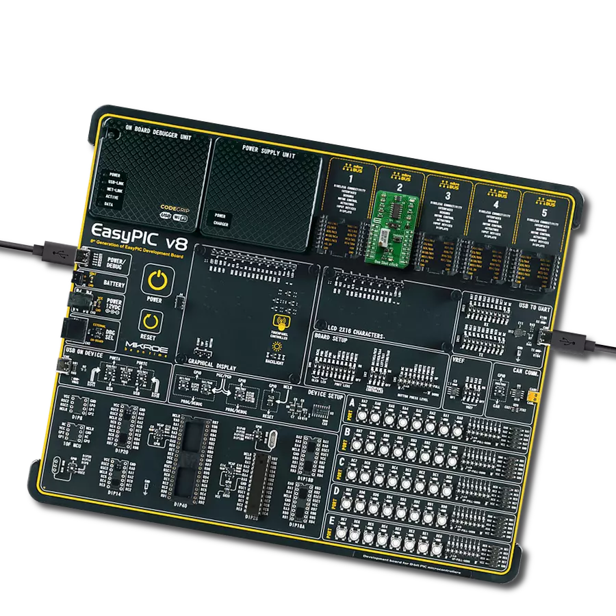
Development board
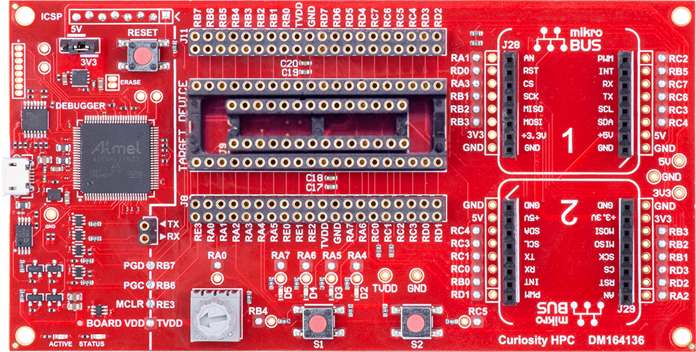
Curiosity HPC, standing for Curiosity High Pin Count (HPC) development board, supports 28- and 40-pin 8-bit PIC MCUs specially designed by Microchip for the needs of rapid development of embedded applications. This board has two unique PDIP sockets, surrounded by dual-row expansion headers, allowing connectivity to all pins on the populated PIC MCUs. It also contains a powerful onboard PICkit™ (PKOB), eliminating the need for an external programming/debugging tool, two mikroBUS™ sockets for Click board™ connectivity, a USB connector, a set of indicator LEDs, push button switches and a variable potentiometer. All
these features allow you to combine the strength of Microchip and Mikroe and create custom electronic solutions more efficiently than ever. Each part of the Curiosity HPC development board contains the components necessary for the most efficient operation of the same board. An integrated onboard PICkit™ (PKOB) allows low-voltage programming and in-circuit debugging for all supported devices. When used with the MPLAB® X Integrated Development Environment (IDE, version 3.0 or higher) or MPLAB® Xpress IDE, in-circuit debugging allows users to run, modify, and troubleshoot their custom software and hardware
quickly without the need for additional debugging tools. Besides, it includes a clean and regulated power supply block for the development board via the USB Micro-B connector, alongside all communication methods that mikroBUS™ itself supports. Curiosity HPC development board allows you to create a new application in just a few steps. Natively supported by Microchip software tools, it covers many aspects of prototyping thanks to many number of different Click boards™ (over a thousand boards), the number of which is growing daily.

Microcontroller Overview
MCU Card / MCU
Architecture
PIC
MCU Memory (KB)
32
Silicon Vendor
Microchip
Pin count
28
RAM (Bytes)
3648
Used MCU Pins
mikroBUS™ mapper
Take a closer look
Click board™ Schematic
Step by step
Project assembly
Start by selecting your development board and Click board™. Begin with the Curiosity HPC as your development board.


Track your results in real time
Application Output
1. Application Output - In Debug mode, the 'Application Output' window enables real-time data monitoring, offering direct insight into execution results. Ensure proper data display by configuring the environment correctly using the provided tutorial.

2. UART Terminal - Use the UART Terminal to monitor data transmission via a USB to UART converter, allowing direct communication between the Click board™ and your development system. Configure the baud rate and other serial settings according to your project's requirements to ensure proper functionality. For step-by-step setup instructions, refer to the provided tutorial.

3. Plot Output - The Plot feature offers a powerful way to visualize real-time sensor data, enabling trend analysis, debugging, and comparison of multiple data points. To set it up correctly, follow the provided tutorial, which includes a step-by-step example of using the Plot feature to display Click board™ readings. To use the Plot feature in your code, use the function: plot(*insert_graph_name*, variable_name);. This is a general format, and it is up to the user to replace 'insert_graph_name' with the actual graph name and 'variable_name' with the parameter to be displayed.

Software Support
Library Description
This library contains API for Clock Gen 3 Click driver.
Key functions:
void clockgen3_set_freq( float freq )- Sets Frequencyvoid clockgen3_config( uint8_t cfg )- Configuration
Open Source
Code example
The complete application code and a ready-to-use project are available through the NECTO Studio Package Manager for direct installation in the NECTO Studio. The application code can also be found on the MIKROE GitHub account.
/*!
 * \file
 * \brief ClockGen3 Click example
 *
 * # Description
 * This example demonstrates the use of Clock Gen 3 Click board.
 *
 * The demo application is composed of two sections :
 *
 * ## Application Init
 * Initializes the driver and configures the Click board.
 *
 * ## Application Task
 * Sets different frequencies every 3 seconds and displays the set frequency
 * on the USB UART.
 *
 * \author MikroE Team
 *
 */
// ------------------------------------------------------------------- INCLUDES

#include "board.h"
#include "log.h"
#include "clockgen3.h"

// ------------------------------------------------------------------ VARIABLES

static clockgen3_t clockgen3;
static log_t logger;

// ------------------------------------------------------ APPLICATION FUNCTIONS

void application_init ( void )
{
    log_cfg_t log_cfg;
    clockgen3_cfg_t cfg;

    /**
     * Logger initialization.
     * Default baud rate: 115200
     * Default log level: LOG_LEVEL_DEBUG
     * @note If USB_UART_RX and USB_UART_TX
     * are defined as HAL_PIN_NC, you will
     * need to define them manually for log to work.
     * See @b LOG_MAP_USB_UART macro definition for detailed explanation.
     */
    LOG_MAP_USB_UART( log_cfg );
    log_init( &logger, &log_cfg );
    log_info( &logger, "---- Application Init ----" );

    // Click initialization.
    clockgen3_cfg_setup( &cfg );
    CLOCKGEN3_MAP_MIKROBUS( cfg, MIKROBUS_1 );
    clockgen3_init( &clockgen3, &cfg );

    clockgen3_config( &clockgen3, CLOCKGEN3_CFG_ON_CLK_180 );
    Delay_ms ( 500 );
}

void application_task ( void )
{
    log_printf( &logger, ">> Set Freq = 12.000 MHz \r\n" );
    clockgen3_set_freq( &clockgen3, 12000.0 );
    Delay_ms ( 1000 );
    Delay_ms ( 1000 );
    Delay_ms ( 1000 );
    log_printf( &logger, ">> Set Freq = 8.000 MHz \r\n" );
    clockgen3_set_freq( &clockgen3, 8000.0 );
    Delay_ms ( 1000 );
    Delay_ms ( 1000 );
    Delay_ms ( 1000 );
    log_printf( &logger, ">> Set Freq = 5.500 MHz \r\n" );
    clockgen3_set_freq( &clockgen3, 5500.0 );
    Delay_ms ( 1000 );
    Delay_ms ( 1000 );
    Delay_ms ( 1000 );
    log_printf( &logger, ">> Set Freq = 2.700 MHz \r\n" );
    clockgen3_set_freq( &clockgen3, 2700.0 );
    Delay_ms ( 1000 );
    Delay_ms ( 1000 );
    Delay_ms ( 1000 );
    log_printf( &logger, ">> Set Freq = 800 KHz \r\n" );
    clockgen3_set_freq( &clockgen3, 800.0 );
    Delay_ms ( 1000 );
    Delay_ms ( 1000 );
    Delay_ms ( 1000 );
    log_printf( &logger, ">> Set Freq = 200 KHz \r\n" );
    clockgen3_set_freq( &clockgen3, 200.0 );
    Delay_ms ( 1000 );
    Delay_ms ( 1000 );
    Delay_ms ( 1000 );
    log_printf( &logger, "---------------------------- \r\n" );
}

int main ( void )
{
    /* Do not remove this line or clock might not be set correctly. */
    #ifdef PREINIT_SUPPORTED
    preinit();
    #endif

    application_init( );

    for ( ; ; )
    {
        application_task( );
    }

    return 0;
}

// ------------------------------------------------------------------------ END
Additional Support
Resources
Category:Clock generator