Seamlessly transform varying frequencies into precise voltage signals with TC9400 and PIC18F2455
Frequency-to-Voltage: Unveiling the magic of signal transformation!

Published Jan 23, 2024
Click board™
Hz To V Click
Dev. board
Curiosity HPC
Compiler
NECTO Studio
MCU
PIC18F2455
Navigate the world of signal analysis with confidence using our frequency-to-voltage solution, offering unparalleled precision in capturing and converting frequency data into voltage signals
A
A
Hardware Overview
How does it work?
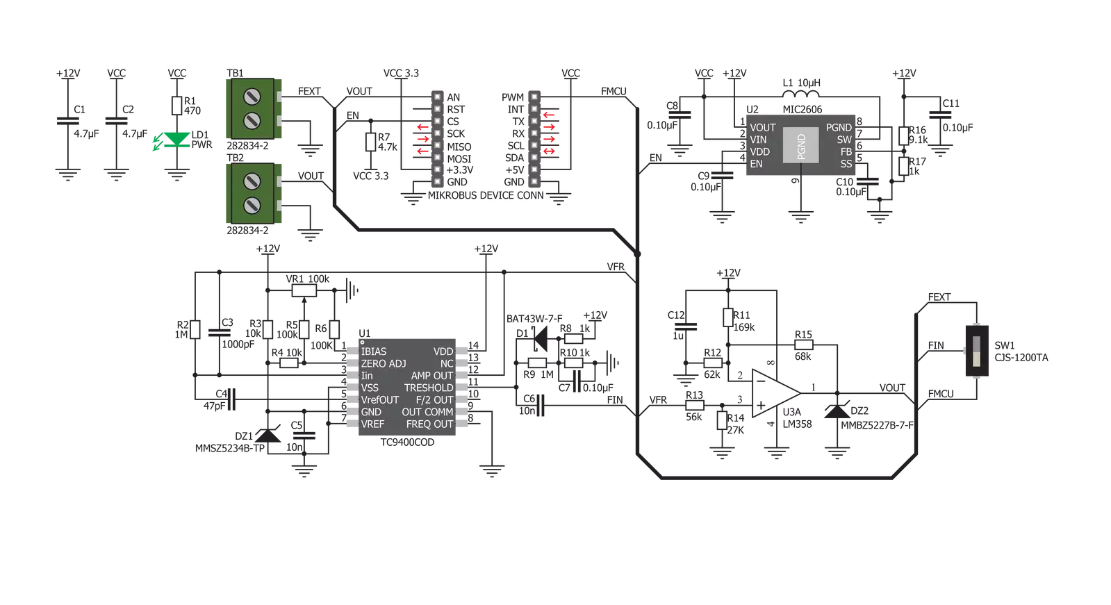
Hz to V Click is based on the TC9400, a voltage-to-frequency and frequency-to-voltage converter from Microchip. It accepts a signal with the frequency within a range between 1kHz and 10kHz on the input and generates DC voltage with the level corresponding to the input frequency, ranging from 0.33V to 3.3V, with a highly linear response. This signal is further passed through the operational amplifier, in order to scale it down to a level acceptable by the MCU. The input signal can be applied either to the PWM pin of the mikroBUS™ or the external input terminal. The input source can be selected with the onboard switch, labeled as INPUT SEL. When Hz to V click is operated for the first time, it needs to be calibrated. The click is equipped with a variable resistor for the offset fine tuning. The following procedure should be followed to calibrate the
device: an input signal with a frequency of 1kHz should be applied to the input. The offset should be adjusted so that a 330mV DC signal appears on the output. Hz to V click is equipped with the input signal terminal (FREQ IN), which is used to connect the signal with a frequency which is in the acceptable range between 1kHz and 10kHz. Besides this signal input terminal, it is possible to select the PWM signal generated by the host MCU as the input, too. INPUT SEL switch can be set so that the PWM pin from the mikroBUS™ is used as the control voltage input. It is recommended that the signal amplitude does not exceed 3.3V. The output terminal (VOLT OUT) is used to output the generated voltage. As already explained, the voltage level depends on the input signal frequency. This generated voltage is also available on the AN pin of the mikroBUS™. The output
signal is passed through the operational amplifier (OPAMP) which is used both as the output buffer and a voltage adjust stage for the output voltage. A well known general purpose operational amplifier LM318 from Texas Instruments is used for this purpose. To provide 12V for the TC9400 and the LM318 OPAMP, Hz to V click employs a boost converter built around the MIC2606, a boost regulator from Microchip, which works at 2MHz. This IC provides 12V for supplying the TC9400 out of 5V routed from the mikroBUS™ socket. The EN pin of the boost regulator is routed to the mikroBUS™ CS pin and it is used to enable power output from the boost regulator, effectively enabling the TC9400 itself. The EN pin is pulled to a HIGH logic level (3.3V) by the onboard resistor.

Features overview
Development board
Curiosity HPC, standing for Curiosity High Pin Count (HPC) development board, supports 28- and 40-pin 8-bit PIC MCUs specially designed by Microchip for the needs of rapid development of embedded applications. This board has two unique PDIP sockets, surrounded by dual-row expansion headers, allowing connectivity to all pins on the populated PIC MCUs. It also contains a powerful onboard PICkit™ (PKOB), eliminating the need for an external programming/debugging tool, two mikroBUS™ sockets for Click board™ connectivity, a USB connector, a set of indicator LEDs, push button switches and a variable potentiometer. All
these features allow you to combine the strength of Microchip and Mikroe and create custom electronic solutions more efficiently than ever. Each part of the Curiosity HPC development board contains the components necessary for the most efficient operation of the same board. An integrated onboard PICkit™ (PKOB) allows low-voltage programming and in-circuit debugging for all supported devices. When used with the MPLAB® X Integrated Development Environment (IDE, version 3.0 or higher) or MPLAB® Xpress IDE, in-circuit debugging allows users to run, modify, and troubleshoot their custom software and hardware
quickly without the need for additional debugging tools. Besides, it includes a clean and regulated power supply block for the development board via the USB Micro-B connector, alongside all communication methods that mikroBUS™ itself supports. Curiosity HPC development board allows you to create a new application in just a few steps. Natively supported by Microchip software tools, it covers many aspects of prototyping thanks to many number of different Click boards™ (over a thousand boards), the number of which is growing daily.

Microcontroller Overview
MCU Card / MCU
Architecture
PIC
MCU Memory (KB)
24
Silicon Vendor
Microchip
Pin count
28
RAM (Bytes)
2048
Used MCU Pins
mikroBUS™ mapper
Take a closer look
Click board™ Schematic
Step by step
Project assembly

Start by selecting your development board and Click board™. Begin with the Curiosity HPC as your development board.


Track your results in real time
Application Output
1. Application Output - In Debug mode, the 'Application Output' window enables real-time data monitoring, offering direct insight into execution results. Ensure proper data display by configuring the environment correctly using the provided tutorial.

2. UART Terminal - Use the UART Terminal to monitor data transmission via a USB to UART converter, allowing direct communication between the Click board™ and your development system. Configure the baud rate and other serial settings according to your project's requirements to ensure proper functionality. For step-by-step setup instructions, refer to the provided tutorial.

3. Plot Output - The Plot feature offers a powerful way to visualize real-time sensor data, enabling trend analysis, debugging, and comparison of multiple data points. To set it up correctly, follow the provided tutorial, which includes a step-by-step example of using the Plot feature to display Click board™ readings. To use the Plot feature in your code, use the function: plot(*insert_graph_name*, variable_name);. This is a general format, and it is up to the user to replace 'insert_graph_name' with the actual graph name and 'variable_name' with the parameter to be displayed.

Software Support
Library Description
This library contains API for Hz To V Click driver.
Key functions:
hztov_read_voltage- Read voltage functionhztov_set_input_frequency- Changing the output voltage function.
Open Source
Code example
The complete application code and a ready-to-use project are available through the NECTO Studio Package Manager for direct installation in the NECTO Studio. The application code can also be found on the MIKROE GitHub account.
/*!
 * \file
 * \brief HzToV Click example
 *
 * # Description
 * This example demonstrates the use of Hz to V Click board.
 *
 * The demo application is composed of two sections :
 *
 * ## Application Init
 * Initializes the driver and enables the Click board.
 *
 * ## Application Task
 * Sets the PWM frequency then reads the voltage from VO pin and logs all data on USB UART.
 *
 * @note
 * In order to set PWM frequency down to 1 kHz, the user will probably need to
 * lower the main MCU clock frequency.
 * The output voltage may vary, depending on the offset potentiometer setting on the Click.
 *
 * \author MikroE Team
 *
 */
// ------------------------------------------------------------------- INCLUDES

#include "board.h"
#include "log.h"
#include "hztov.h"

// ------------------------------------------------------------------ VARIABLES

static hztov_t hztov;
static log_t logger;
static float voltage;
static uint16_t fin;

// ------------------------------------------------------ APPLICATION FUNCTIONS

void application_init ( void )
{
    log_cfg_t log_cfg;
    hztov_cfg_t cfg;

    /**
     * Logger initialization.
     * Default baud rate: 115200
     * Default log level: LOG_LEVEL_DEBUG
     * @note If USB_UART_RX and USB_UART_TX
     * are defined as HAL_PIN_NC, you will
     * need to define them manually for log to work.
     * See @b LOG_MAP_USB_UART macro definition for detailed explanation.
     */
    LOG_MAP_USB_UART( log_cfg );
    log_init( &logger, &log_cfg );
    log_info( &logger, "---- Application Init ----" );

    //  Click initialization.

    hztov_cfg_setup( &cfg );
    HZTOV_MAP_MIKROBUS( cfg, MIKROBUS_1 );
    hztov_init( &hztov, &cfg );

    hztov_set_enable ( &hztov, HZTOV_ENABLE );

    fin = HZTOV_MIN_FREQ;

    Delay_ms ( 100 );
}

void application_task ( void )
{
    if ( fin > HZTOV_MAX_FREQ )
        fin = HZTOV_MIN_FREQ;
    hztov_set_input_frequency( &hztov, fin );
    Delay_ms ( 1000 );
    log_printf( &logger, "Frequency: %u Hz \r\n", fin );
    voltage = 0;
    for ( uint8_t cnt = 0; cnt < 100; cnt++ )
    {
        voltage += hztov_read_voltage( &hztov );
    }
    log_printf( &logger, "Voltage: %.2f V \r\n", voltage / 100.0 );
    log_printf( &logger, "-------------------\r\n" );

    fin += 1000;
    Delay_ms ( 1000 );
    Delay_ms ( 1000 );
}

int main ( void )
{
    /* Do not remove this line or clock might not be set correctly. */
    #ifdef PREINIT_SUPPORTED
    preinit();
    #endif

    application_init( );

    for ( ; ; )
    {
        application_task( );
    }

    return 0;
}


// ------------------------------------------------------------------------ END


