Experience powerful sound without compromise with TPA3128D2 and PIC18F57Q43
Unleash the sonic potential

Published Feb 13, 2024
Click board™
2x30W Amp Click
Development board
Curiosity Nano with PIC18F57Q43
Compiler
NECTO Studio
MCU
PIC18F57Q43
Whether you're a music enthusiast, a DIY audio project lover, or a professional sound designer, the 2x30W Amp Click is perfect for amplifying audio signals compactly and efficiently
A
A
Hardware Overview
How does it work?
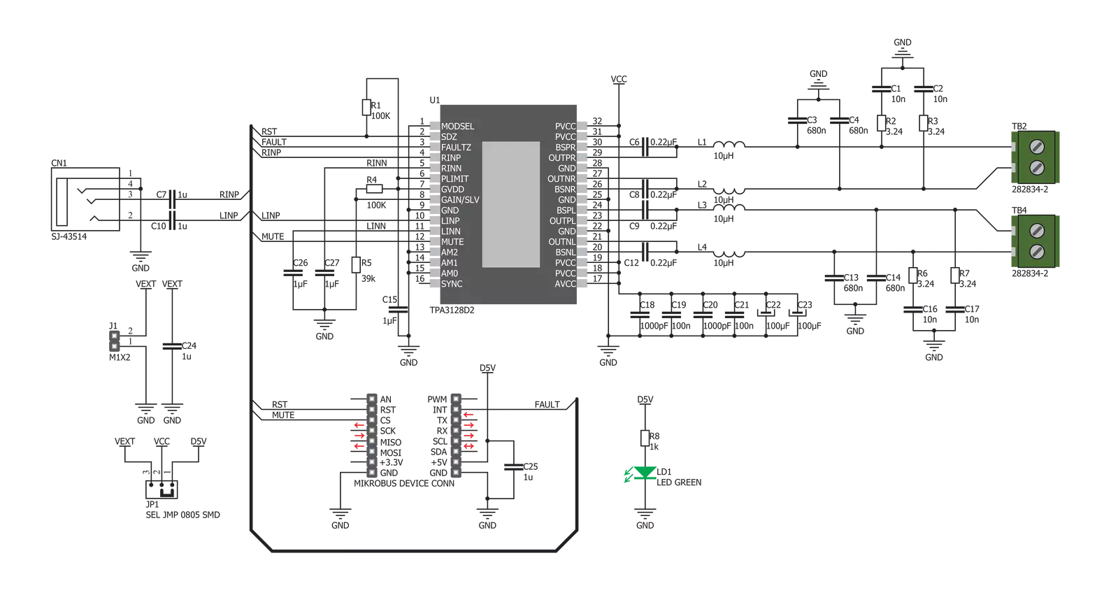
2x30W Amp Click is based on the TPA3128, 2x30-W class-D amplifier with low idle power dissipation from Texas Instruments. The most important characteristic of this IC is its output efficiency, which reduces the need for bulky heat sinks, usually associated with audio amplifiers. This is accomplished by switching MOSFET outputs, which have very low RDSON, as low as 90 mΩ. ClassD amplifiers are way more efficient by design than class A or AB amplifiers. Class D amplifier working principles are based on the switching characteristic of the transistors rather than the linear characteristic used for the A/AB class amplifiers. The audio signal is encoded into a PWM signal with a fixed amplitude. An output signal is restored through the LC filter and the speaker itself. Since the basis of this principle is switching the signal, and the transistors are either fully ON or fully OFF, they spend very little time in the linear region and dissipate very little power. Using low RDSON MOSFETs becomes possible and desirable so that the efficiency goes up to 90% and over. 2x30W Amp click is designed to work with two channels of a single-sided audio source, connected via the 3.5mm stereo audio jack provided on board. The Click board™ is equipped with a connector for the external power source.
By default, the 2x30 Amp click is supplied via the mikroBUS™ 5V rail, which limits the output power. An adequate external power supply should be used for the full output power. The TPA3128 IC can handle up to 26V. The onboard SMD jumper should be switched to the desired position (EXT or 5V) to select operation via the external power supply. If the EXT position is selected, the external power supply should be connected via the 1x2 header on the side of the Click board™, labeled as VEXT. The connected speaker impedance should not be less than 4Ω. The speakers can be connected via two edge connectors, with clearly labeled input ports: L+ and L- for connecting the left speaker's positive and negative terminals; R+ and R- for connecting the right speaker's positive and negative terminals. Care should be taken to dimension the speakers according to the maximum output power of the amplifier. The amplifier has a fixed gain of 32dB, determined by two resistors labeled R4 and R5 on the provided schematic. The RST pin of the mikroBUS™ is routed to the SDZ pin of the TPA3128 IC. Setting this pin to a LOW logic level will set the TPA3128 IC in the shutdown mode, with its output stage set to a high impedance (Hi-Z), reducing the idle current to a minimum.
Pulling the SDZ (RST) pin to a LOW logic level before disconnecting the power from the Click board™ to avoid audible power-off clicks is a good practice. The onboard resistor pulls the RST pin up to a HIGH logic level. Another way to mute the speakers is by pulling the MUTE pin to a HIGH logic level. This pin is routed to the CS pin of the mikroBUS™ and labeled as the MT. Pulling this pin to a HIGH logic level will also set the output stage to a Hi-Z, but it will perform a muting function only, thus muting the IC faster than the complete shutdown with the SDZ pin. This function is useful if used in conjunction with the FAULT pin, allowing power-up in a muted state when there is a problem on the output stage. The FAULTZ pin is routed to the INT pin of the mikroBUS™ and labeled as the FLT. It is used to signalize the fault condition (overtemperature, output DC offset detection) to the host MCU. It is active low and can trigger an interrupt request on the host MCU so that the proper action can be taken. The Click board™ uses only GPIO pins, which is extremely simple. However, the Click board™ comes equipped with a library containing easy-to-use functions and an example code that can be used, as a reference, for further development.

Features overview
Development board
PIC18F57Q43 Curiosity Nano evaluation kit is a cutting-edge hardware platform designed to evaluate microcontrollers within the PIC18-Q43 family. Central to its design is the inclusion of the powerful PIC18F57Q43 microcontroller (MCU), offering advanced functionalities and robust performance. Key features of this evaluation kit include a yellow user LED and a responsive
mechanical user switch, providing seamless interaction and testing. The provision for a 32.768kHz crystal footprint ensures precision timing capabilities. With an onboard debugger boasting a green power and status LED, programming and debugging become intuitive and efficient. Further enhancing its utility is the Virtual serial port (CDC) and a debug GPIO channel (DGI
GPIO), offering extensive connectivity options. Powered via USB, this kit boasts an adjustable target voltage feature facilitated by the MIC5353 LDO regulator, ensuring stable operation with an output voltage ranging from 1.8V to 5.1V, with a maximum output current of 500mA, subject to ambient temperature and voltage constraints.

Microcontroller Overview
MCU Card / MCU

Architecture
PIC
MCU Memory (KB)
128
Silicon Vendor
Microchip
Pin count
48
RAM (Bytes)
8196
You complete me!
Accessories
Curiosity Nano Base for Click boards is a versatile hardware extension platform created to streamline the integration between Curiosity Nano kits and extension boards, tailored explicitly for the mikroBUS™-standardized Click boards and Xplained Pro extension boards. This innovative base board (shield) offers seamless connectivity and expansion possibilities, simplifying experimentation and development. Key features include USB power compatibility from the Curiosity Nano kit, alongside an alternative external power input option for enhanced flexibility. The onboard Li-Ion/LiPo charger and management circuit ensure smooth operation for battery-powered applications, simplifying usage and management. Moreover, the base incorporates a fixed 3.3V PSU dedicated to target and mikroBUS™ power rails, alongside a fixed 5.0V boost converter catering to 5V power rails of mikroBUS™ sockets, providing stable power delivery for various connected devices.

Used MCU Pins
mikroBUS™ mapper
Take a closer look
Schematic
Step by step
Project assembly

Start by selecting your development board and Click board™. Begin with the Curiosity Nano with PIC18F57Q43 as your development board.


Track your results in real time
Application Output
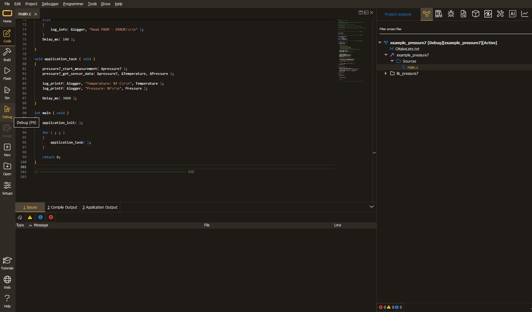
After loading the code example, pressing the "DEBUG" button builds and programs it on the selected setup.
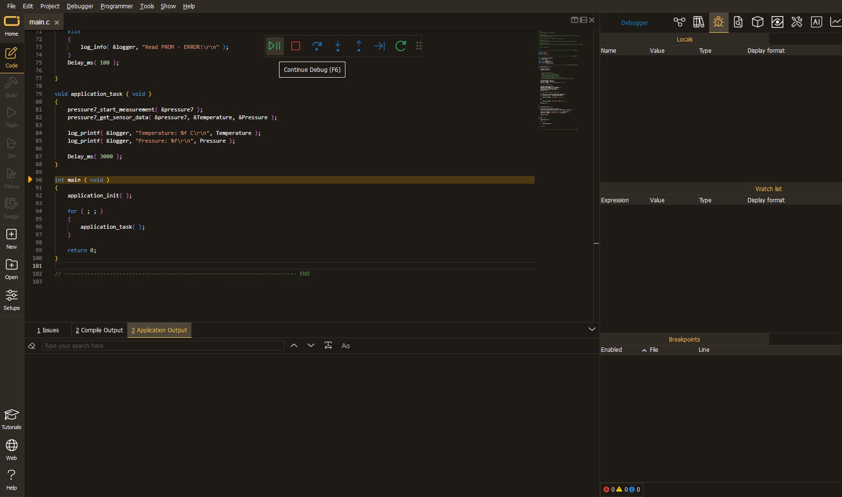
After programming is completed, a header with buttons for various actions available in the IDE appears. By clicking the green "PLAY "button, we start reading the results achieved with Click board™.
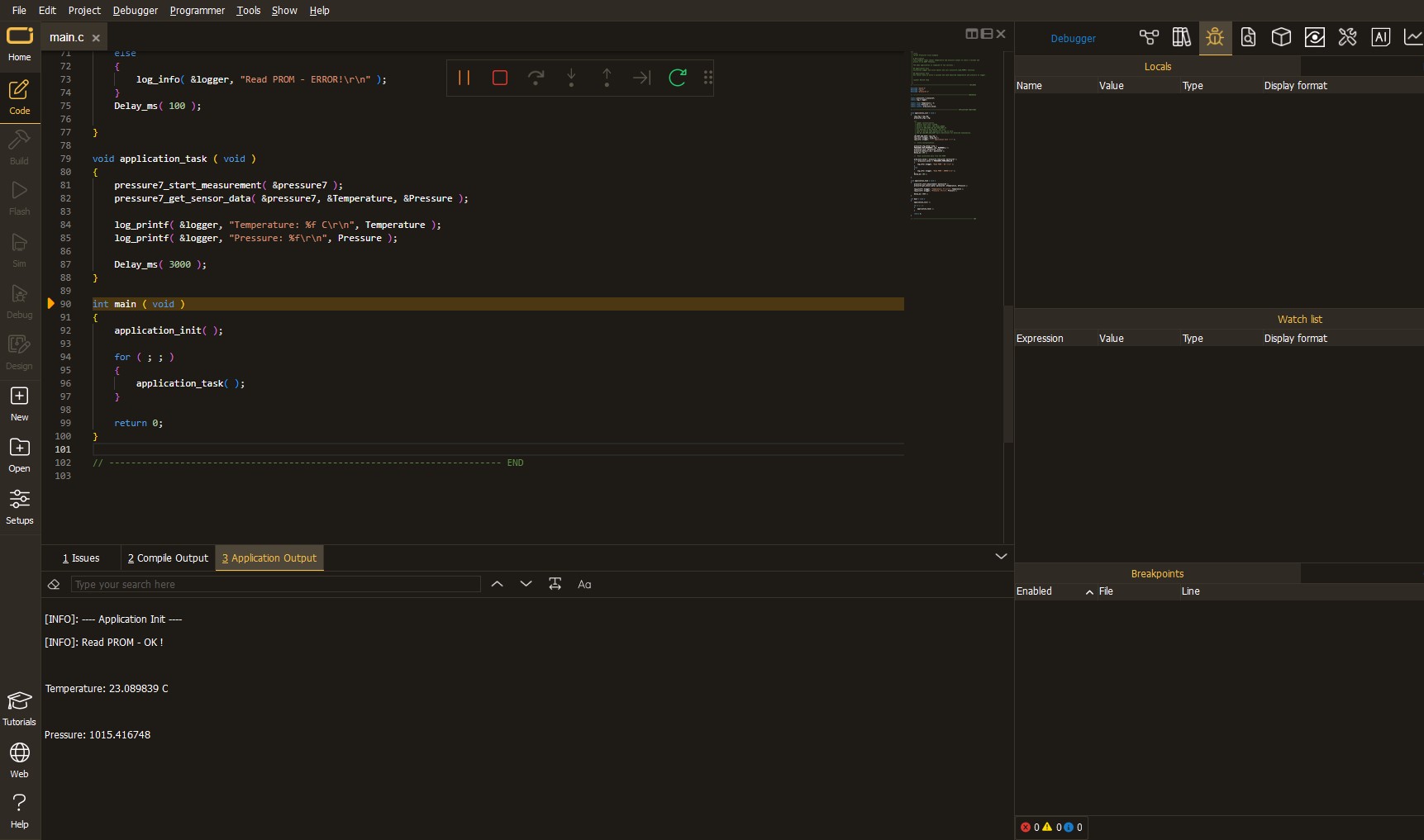
Upon completion of programming, the Application Output tab is automatically opened, where the achieved result can be read. In case of an inability to perform the Debug function, check if a proper connection between the MCU used by the setup and the CODEGRIP programmer has been established. A detailed explanation of the CODEGRIP-board connection can be found in the CODEGRIP User Manual. Please find it in the RESOURCES section.
Software Support
Library Description
This library contains API for 2x30W Amp Click driver.
Key functions:
c2x30wamp_enable- Device Enable functionc2x30wamp_mute- Device Mute functionc2x30wamp_check_diagnostic- Diagnostic Check function
Open Source
Code example
This example can be found in NECTO Studio. Feel free to download the code, or you can copy the code below.
/*!
 * \file
 * \brief c2x30W Amp Click example
 *
 * # Description
 * This application is audio amplifier.
 *
 * The demo application is composed of two sections :
 *
 * ## Application Init
 * Initializes GPIO driver and enables the device.
 *
 * ## Application Task
 * Mute output for a period of 3 seconds, then keep it unmuted for a period of 10 seconds.
 * After that, checks if over current fault, over temperature fault or too high DC offset fault occurred.
 *
 * ## NOTE
 * When under or over voltage condition occurres the output goes to high impedance state,
 * but the FAULT pin will not be asserted.
 *
 * \author MikroE Team
 *
 */
// ------------------------------------------------------------------- INCLUDES

#include "board.h"
#include "log.h"
#include "c2x30wamp.h"

// ------------------------------------------------------------------ VARIABLES

static c2x30wamp_t c2x30wamp;
static log_t logger;

// ------------------------------------------------------ APPLICATION FUNCTIONS

void application_init ( void )
{
    log_cfg_t log_cfg;
    c2x30wamp_cfg_t cfg;

    /**
     * Logger initialization.
     * Default baud rate: 115200
     * Default log level: LOG_LEVEL_DEBUG
     * @note If USB_UART_RX and USB_UART_TX
     * are defined as HAL_PIN_NC, you will
     * need to define them manually for log to work.
     * See @b LOG_MAP_USB_UART macro definition for detailed explanation.
     */
    LOG_MAP_USB_UART( log_cfg );
    log_init( &logger, &log_cfg );
    log_info(&logger, "---- Application Init ----");

    //  Click initialization.

    c2x30wamp_cfg_setup( &cfg );
    C2X30WAMP_MAP_MIKROBUS( cfg, MIKROBUS_1 );
    c2x30wamp_init( &c2x30wamp, &cfg );

    c2x30wamp_enable( &c2x30wamp, C2X30WAMP_ENABLE );
    log_printf( &logger, "2x30W AMP is initialized \r\n" );
    Delay_ms( 200 );
}

void application_task ( void )
{
    c2x30wamp_mute( &c2x30wamp, C2X30WAMP_MUTE );
    log_printf( &logger, "---------------------- \r\n" );
    log_printf( &logger, "MUTE \r\n" );
    Delay_ms( 3000 );
    c2x30wamp_mute( &c2x30wamp, C2X30WAMP_UNMUTE );
    log_printf( &logger, "---------------------- \r\n" );
    log_printf( &logger, "UNMUTE \r\n" );
    Delay_ms( 10000 );

    uint8_t fault_check = c2x30wamp_check_diagnostic( &c2x30wamp );

    if ( fault_check == 0 )
    {
        log_printf( &logger, "Fault condition! \r\n" );
    }
}

void main ( void )
{
    application_init( );

    for ( ; ; )
    {
        application_task( );
    }
}

// ------------------------------------------------------------------------ END


