Enhance your system performance with AD74412R and PIC18F57Q43
Compact yet powerful

Published Feb 13, 2024
Click board™
AD-SWIO Click
Dev. board
Curiosity Nano with PIC18F57Q43
Compiler
NECTO Studio
MCU
PIC18F57Q43
The game-changer for applications demanding simultaneous ADC and DAC functionality
A
A
Hardware Overview
How does it work?
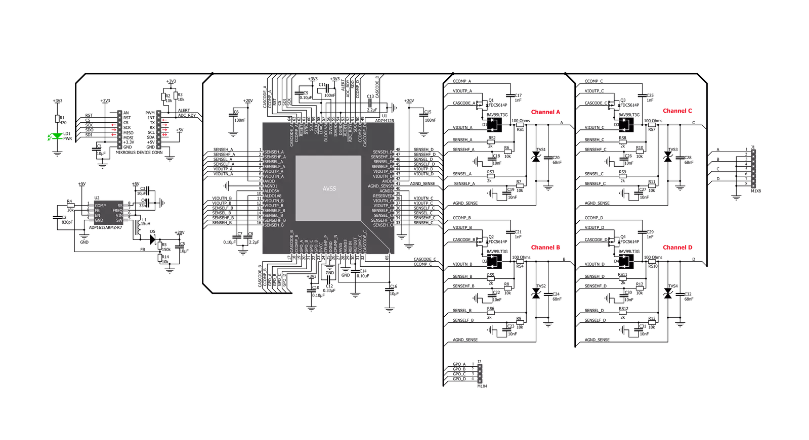
AD-SWIO Click is based on AD74412R, a 16-bit analog-to-digital converter (ADC), and a 13-bit digital-to-analog converter (DAC) from Analog Devices. There are several modes related to the AD74412R. These modes are voltage output, current output, voltage input, externally powered current input, loop-powered current input, external RTD measurement, digital input logic, and loop-powered digital input. The ADC can measure the voltage across the 100Ω RSENSE or at each channel's I/OP_x screw terminal. In high impedance mode, the ADC, by default, measures the voltage across the screw terminals (I/OP_x to I/ON_x) in a 0V to 10V range. The ADC also provides diagnostic information on user-selectable inputs such as supplies, internal die temperature, reference, and regulators. The AD-SWIO Click has four GPO-x pins, one per channel (GPO-A, GPO-B, GPO-C, GPO-D).
Each channel GPO-x pin can be configured to the logic outputs of the digital input functions or a logic high or low output. The GPO-x pins can be set via the GPO_SELECT bits within the GPO_CONFIGx registers. The Click board™ also contains an LVIN ( Low Voltage Input) pin, the measurement voltage range on this pin is 0V to 2.5V. The AD74412R has four 13-bit DACs, one per channel. Each DAC core is a 13-bit string DAC. The architecture structure consists of a string of resistors, each with a value of R. The digital input code loaded to the DAC_CODEx registers determines which string node the voltage is tapped off from and fed into the output amplifier. This architecture is inherently monotonic and linear. The AD74412R has short-circuited limit in voltage output mode that is programmable per channel. The circuit minimizes glitching on the I/OP_x screw terminal when the AVDD
supply is ramping, or the use case configuration is changed. This short-circuit limit you can regulate with a positive analog supply on the AVDD pin, Output voltage on AD-SWIO 2 Click is limited to +20V. The AD-SWIO 2 Click is equipped with the ADP1613 step-up dc-to-dc switching converter from Analog Devices with an integrated power switch capable of providing an output voltage as high as 20V. This Click board™ can only be operated with a 3.3V logic voltage level. The board must perform appropriate logic voltage level conversion before using MCUs with different logic levels. However, the Click board™ comes equipped with a library containing functions and an example code that can be used as a reference for further development.

Features overview
Development board
PIC18F57Q43 Curiosity Nano evaluation kit is a cutting-edge hardware platform designed to evaluate microcontrollers within the PIC18-Q43 family. Central to its design is the inclusion of the powerful PIC18F57Q43 microcontroller (MCU), offering advanced functionalities and robust performance. Key features of this evaluation kit include a yellow user LED and a responsive
mechanical user switch, providing seamless interaction and testing. The provision for a 32.768kHz crystal footprint ensures precision timing capabilities. With an onboard debugger boasting a green power and status LED, programming and debugging become intuitive and efficient. Further enhancing its utility is the Virtual serial port (CDC) and a debug GPIO channel (DGI
GPIO), offering extensive connectivity options. Powered via USB, this kit boasts an adjustable target voltage feature facilitated by the MIC5353 LDO regulator, ensuring stable operation with an output voltage ranging from 1.8V to 5.1V, with a maximum output current of 500mA, subject to ambient temperature and voltage constraints.

Microcontroller Overview
MCU Card / MCU

Architecture
PIC
MCU Memory (KB)
128
Silicon Vendor
Microchip
Pin count
48
RAM (Bytes)
8196
You complete me!
Accessories
Curiosity Nano Base for Click boards is a versatile hardware extension platform created to streamline the integration between Curiosity Nano kits and extension boards, tailored explicitly for the mikroBUS™-standardized Click boards and Xplained Pro extension boards. This innovative base board (shield) offers seamless connectivity and expansion possibilities, simplifying experimentation and development. Key features include USB power compatibility from the Curiosity Nano kit, alongside an alternative external power input option for enhanced flexibility. The onboard Li-Ion/LiPo charger and management circuit ensure smooth operation for battery-powered applications, simplifying usage and management. Moreover, the base incorporates a fixed 3.3V PSU dedicated to target and mikroBUS™ power rails, alongside a fixed 5.0V boost converter catering to 5V power rails of mikroBUS™ sockets, providing stable power delivery for various connected devices.

Used MCU Pins
mikroBUS™ mapper
Take a closer look
Click board™ Schematic
Step by step
Project assembly

Start by selecting your development board and Click board™. Begin with the Curiosity Nano with PIC18F57Q43 as your development board.


Track your results in real time
Application Output
1. Application Output - In Debug mode, the 'Application Output' window enables real-time data monitoring, offering direct insight into execution results. Ensure proper data display by configuring the environment correctly using the provided tutorial.

2. UART Terminal - Use the UART Terminal to monitor data transmission via a USB to UART converter, allowing direct communication between the Click board™ and your development system. Configure the baud rate and other serial settings according to your project's requirements to ensure proper functionality. For step-by-step setup instructions, refer to the provided tutorial.

3. Plot Output - The Plot feature offers a powerful way to visualize real-time sensor data, enabling trend analysis, debugging, and comparison of multiple data points. To set it up correctly, follow the provided tutorial, which includes a step-by-step example of using the Plot feature to display Click board™ readings. To use the Plot feature in your code, use the function: plot(*insert_graph_name*, variable_name);. This is a general format, and it is up to the user to replace 'insert_graph_name' with the actual graph name and 'variable_name' with the parameter to be displayed.

Software Support
Library Description
This library contains API for AD-SWIO Click driver.
Key functions:
adswio_status_pin_ready- This function checks the status of the ready pin.adswio_get_conv_results- This function allows user to get the converted results of the selected channel.
Open Source
Code example
The complete application code and a ready-to-use project are available through the NECTO Studio Package Manager for direct installation in the NECTO Studio. The application code can also be found on the MIKROE GitHub account.
/*!
 * \file
 * \brief AdSwio Click example
 *
 * # Description
 * This Click provides a fully integrated single chip solution for input and output operation.
 * The AD-SWIO Click contains four 13-bit DACs, one per chanal, and 16-bit Σ-∆ ADC.
 * These options give a lot of flexibility in choosing functionality for analog output,
 * analog input, digital input, resistance temperature detector (RTD), and thermocouple
 * measurements integrated into a single chip solution with a serial peripheral interface (SPI).
 *
 * The demo application is composed of two sections :
 *
 * ## Application Init
 * Performs a hardware reset of the Click board and
 * executes a default configuration that enables channel A and sets it to measure voltage
 * input in the range from 0V to 10V, with 4800 SPS.
 *
 * ## Application Task
 * Waits for the data ready and then reads the results of ADC conversion from channel A
 * and if response is ok, then prints the results on the uart console.
 *
 * ## Additional Functions
 *
 * - void application_default_handler ( uint8_t *err_msg ) - Sends an error report messages from Click
 * driver to initialized console module. It must be set using adswio2_set_handler function.
 *
 *
 * \author MikroE Team
 *
 */
// ------------------------------------------------------------------- INCLUDES

#include "board.h"
#include "log.h"
#include "adswio.h"

// ------------------------------------------------------------------ VARIABLES

static adswio_t adswio;
static log_t logger;

static uint8_t adswio_rdy;
static adswio_err_t adswio_err;
static uint16_t adswio_ch_a;
static float adswio_res;

const uint16_t ADSWIO_RANGE_VOLT_MV = 10000;
const uint32_t ADSWIO_RANGE_RESOLUTION = 65536;

// ------------------------------------------------------ ADDITIONAL FUNCTIONS

void application_default_handler ( uint8_t *err_msg )
{
    char *err_ptr = err_msg;

    log_printf( &logger, "\r\n" );
    log_printf( &logger, "[ERROR] : %s", err_ptr );
    log_printf( &logger, "\r\n" );
}

// ------------------------------------------------------ APPLICATION FUNCTIONS

void application_init ( void )
{
    log_cfg_t log_cfg;
    adswio_cfg_t cfg;

    /**
     * Logger initialization.
     * Default baud rate: 115200
     * Default log level: LOG_LEVEL_DEBUG
     * @note If USB_UART_RX and USB_UART_TX
     * are defined as HAL_PIN_NC, you will
     * need to define them manually for log to work.
     * See @b LOG_MAP_USB_UART macro definition for detailed explanation.
     */
    LOG_MAP_USB_UART( log_cfg );
    log_init( &logger, &log_cfg );
    log_info( &logger, "---- Application Init ----" );

    //  Click initialization.

    adswio_cfg_setup( &cfg );
    ADSWIO_MAP_MIKROBUS( cfg, MIKROBUS_1 );
    adswio_init( &adswio, &cfg );
    Delay_ms ( 100 );

    adswio_default_cfg( &adswio );
    Delay_ms ( 1000 );

    adswio_rdy  = DUMMY;
    adswio_ch_a = DUMMY;
    adswio_res  = DUMMY;
    adswio_err  = ADSWIO_ERR_STATUS_OK;

    log_printf( &logger, " AD-SWIO Click initialization done \r\n");
    log_printf( &logger, "************************************\r\n");
}

void application_task ( void )
{
    uint16_t timeout = 0;
    do
    {
        Delay_1ms( );
        timeout++;
        adswio_rdy = adswio_status_pin_ready( &adswio );
        if ( timeout > 3000 )
        {
            timeout = 0;
            log_printf( &logger, " Reinitializing...");
            adswio_default_cfg( &adswio );
            log_printf( &logger, "Done\r\n");
        }
    }
    while ( adswio_rdy != 0 );

    adswio_err = adswio_get_conv_results( &adswio, ADSWIO_SETUP_CONV_EN_CHA, &adswio_ch_a );

    if ( adswio_err == ADSWIO_ERR_STATUS_OK )
    {
        adswio_res = adswio_ch_a;
        adswio_res /= ADSWIO_RANGE_RESOLUTION;
        adswio_res *= ADSWIO_RANGE_VOLT_MV;
        adswio_ch_a = adswio_res;

        log_printf( &logger, " Voltage from channel A: %d mV\r\n", adswio_ch_a );

        log_printf( &logger, "-----------------------------------\r\n\r\n" );
        Delay_ms ( 200 );
    }
}

int main ( void )
{
    /* Do not remove this line or clock might not be set correctly. */
    #ifdef PREINIT_SUPPORTED
    preinit();
    #endif

    application_init( );

    for ( ; ; )
    {
        application_task( );
    }

    return 0;
}


// ------------------------------------------------------------------------ END


