Convert digital data streams into analog signals with DAC8554 and ATmega328P
Where data shapes analog potential
Published Feb 14, 2024
Click board™
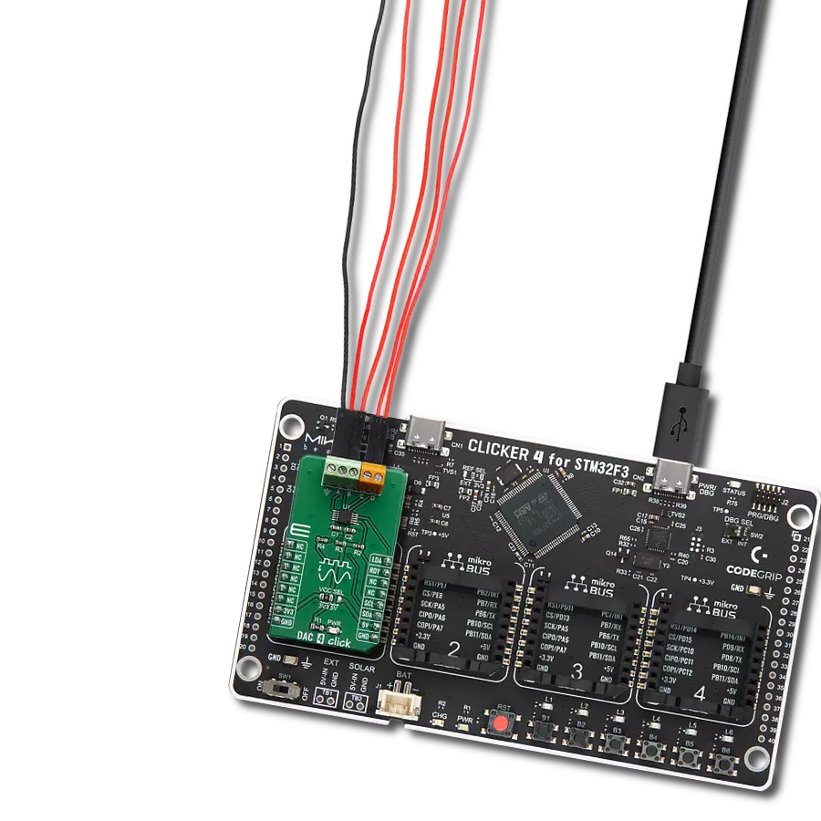
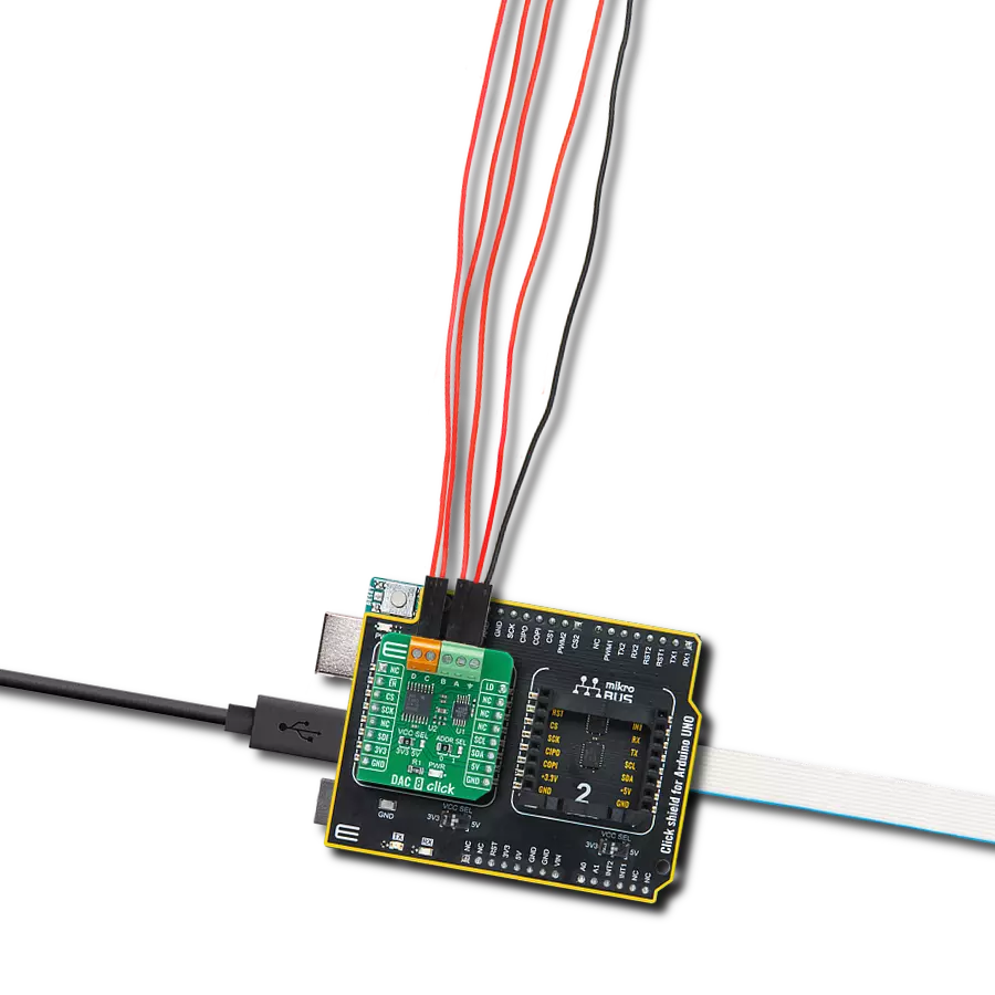
DAC 8 Click
Dev. board
Arduino UNO Rev3
Compiler
NECTO Studio
MCU
ATmega328P
Experience the synergy of precision and transformation with our DAC solution
A
A
Hardware Overview
How does it work?
DAC 8 Click is based on the DAC8554IPWR, a 16-bit QUAD channel, ultra-low glitch, voltage-output digital to analog converter from Texas Instruments. It offers good linearity, exceptionally low glitch, and it has high precision output amplifier that allows rail-to-rail output swing over a wide range of supply voltage. What this component additionally has is a Power-On reset function, which ensures that DAC outputs power-up at zero-scale and remains there until a proper write operation occurs. Also, it provides a power-down feature that reduces the current consumption to 175nA per channel. To achieve a fully flexible range of the DAC8554IPWR, an external voltage reference is made user-programmable. For this purpose, the Click board™ uses another DAC, DAC60501MDGSR, 12-bit DAC from Texas Instruments, whose output is brought to
the VREF pin of the DAC8554IPWR. That way, the reference voltage of the DAC8554IPWR can be set at any value between 0V and 5V, provides high precision and low power consumption as well. That makes the DAC 8 Click fully customizable solution, well suited for applications where the maximum precision from the output 16-bit DAC is needed. DAC60501MDGSR uses the I2C serial interface to communicate with the MCU and operates at clock rate up to 100kHz, with selectable I2C address through ADDR SEL jumper. The DAC 6 Click communicates with MCU using the 3-Wire SPI serial interface that is compatible with standard SPI, QSPI™, MICROWIRE™ and operates at clock rates up to 50 MHz. Additional functionality such as software simultaneous update capability is implemented and routed at the PWM pin of the
mikroBUS™, which allows when new data enter the device, all of DAC outputs can be updated simultaneously and synchronously with the clock. It also possesses enable function routed at CS pin of the mikroBUS™ that is used to connect the SPI interface to the serial port. This Click Board™ is designed to be operated with both 3.3V and 5V logic levels. The onboard SMD jumper labeled as VCC SEL allows voltage selection for interfacing with both 3.3V and 5V MCUs. More information about the DAC8554IPWR’s functionality, electrical specifications, and typical performance can be found in the attached datasheet. However, the Click board™ comes equipped with a library that contains easy-to-use functions, and a usage example that can be used as a reference for the development.

Features overview
Development board
Arduino UNO is a versatile microcontroller board built around the ATmega328P chip. It offers extensive connectivity options for various projects, featuring 14 digital input/output pins, six of which are PWM-capable, along with six analog inputs. Its core components include a 16MHz ceramic resonator, a USB connection, a power jack, an
ICSP header, and a reset button, providing everything necessary to power and program the board. The Uno is ready to go, whether connected to a computer via USB or powered by an AC-to-DC adapter or battery. As the first USB Arduino board, it serves as the benchmark for the Arduino platform, with "Uno" symbolizing its status as the
first in a series. This name choice, meaning "one" in Italian, commemorates the launch of Arduino Software (IDE) 1.0. Initially introduced alongside version 1.0 of the Arduino Software (IDE), the Uno has since become the foundational model for subsequent Arduino releases, embodying the platform's evolution.

Microcontroller Overview
MCU Card / MCU

Architecture
AVR
MCU Memory (KB)
32
Silicon Vendor
Microchip
Pin count
28
RAM (Bytes)
2048
You complete me!
Accessories
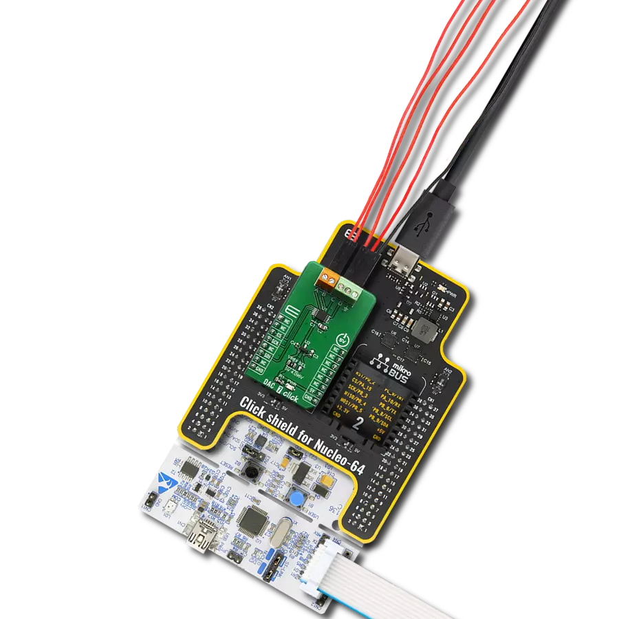
Click Shield for Arduino UNO has two proprietary mikroBUS™ sockets, allowing all the Click board™ devices to be interfaced with the Arduino UNO board without effort. The Arduino Uno, a microcontroller board based on the ATmega328P, provides an affordable and flexible way for users to try out new concepts and build prototypes with the ATmega328P microcontroller from various combinations of performance, power consumption, and features. The Arduino Uno has 14 digital input/output pins (of which six can be used as PWM outputs), six analog inputs, a 16 MHz ceramic resonator (CSTCE16M0V53-R0), a USB connection, a power jack, an ICSP header, and reset button. Most of the ATmega328P microcontroller pins are brought to the IO pins on the left and right edge of the board, which are then connected to two existing mikroBUS™ sockets. This Click Shield also has several switches that perform functions such as selecting the logic levels of analog signals on mikroBUS™ sockets and selecting logic voltage levels of the mikroBUS™ sockets themselves. Besides, the user is offered the possibility of using any Click board™ with the help of existing bidirectional level-shifting voltage translators, regardless of whether the Click board™ operates at a 3.3V or 5V logic voltage level. Once you connect the Arduino UNO board with our Click Shield for Arduino UNO, you can access hundreds of Click boards™, working with 3.3V or 5V logic voltage levels.

Used MCU Pins
mikroBUS™ mapper
Take a closer look
Click board™ Schematic

Step by step
Project assembly

Start by selecting your development board and Click board™. Begin with the Arduino UNO Rev3 as your development board.


Software Support
Library Description
DAC 8 Click demo application is developed using the NECTO Studio, ensuring compatibility with mikroSDK's open-source libraries and tools. Designed for plug-and-play implementation and testing, the demo is fully compatible with all development, starter, and mikromedia boards featuring a mikroBUS™ socket.
Example Description
This Click carries 12-bit buffered Digital-to-Analog Converter. It converts digital value to the corresponding voltage level using external voltage reference.
Key functions:
dac8_cfg_setup- Config Object Initialization function.dac8_init- Initialization function.dac8_device_config- Output digital-to-analog converter on DAC 8 Click board.dac8_load_dac- Buffers of all channels must be loaded with desired data before call Load DAC function.dac8_set_vref- With Precision Internal Reference on DAC 8 Click board.
Application Init
Initialization driver enables - I2C. Configure DAC60501: executes call software reset, disable sync and internal reference and disable Power-down mode, the set reference voltage is internally divided by a factor of 2, amplifier for corresponding DAC has a gain of 2. Initialization driver enables - SPI, enable DAC8554, also write log.
Application Task
This is an example that demonstrates the use of the DAC 8 Click board. DAC 8 board changeing output values: Channel A ~ 2500 mV, Channel B ~ 1250 mV, Channel C ~ 625 mV, Channel D ~ 312 mV. All data logs write on USB uart changes every 5 sec.
Open Source
Code example
The complete application code and a ready-to-use project are available through the NECTO Studio Package Manager for direct installation in the NECTO Studio. The application code can also be found on the MIKROE GitHub account.
/*!
 * \file
 * \brief Dac8 Click example
 *
 * # Description
 * This Click carries 12-bit buffered Digital-to-Analog Converter. It converts digital value to
 * the corresponding voltage level using external voltage reference.
 *
 * The demo application is composed of two sections :
 *
 * ## Application Init
 * Initialization driver enables - I2C.
 * Configure DAC60501: executes call software reset, disable sync and internal reference and
 * disable Power-down mode, the set reference voltage is internally divided by a factor of 2,
 * amplifier for corresponding DAC has a gain of 2.
 * Initialization driver enables - SPI, enable DAC8554, also write log.
 *
 * ## Application Task
 * This is an example that demonstrates the use of the DAC 8 Click board.
 * DAC 8 board changeing output values:
 * Channel A ~ 2500 mV, Channel B ~ 1250 mV,
 * Channel C ~  625 mV, Channel D ~  312 mV.
 * All data logs write on USB uart changes every 5 sec.
 *
 *
 * \author MikroE Team
 *
 */
// ------------------------------------------------------------------- INCLUDES

#include "board.h"
#include "log.h"
#include "dac8.h"

// ------------------------------------------------------------------ VARIABLES

static dac8_t dac8;
static log_t logger;

dac8_cfg_data_t cfg_dac;

// ------------------------------------------------------ APPLICATION FUNCTIONS

void application_init ( void )
{
    log_cfg_t log_cfg;
    dac8_cfg_t cfg;

    /**
     * Logger initialization.
     * Default baud rate: 115200
     * Default log level: LOG_LEVEL_DEBUG
     * @note If USB_UART_RX and USB_UART_TX
     * are defined as HAL_PIN_NC, you will
     * need to define them manually for log to work.
     * See @b LOG_MAP_USB_UART macro definition for detailed explanation.
     */
    LOG_MAP_USB_UART( log_cfg );
    log_init( &logger, &log_cfg );
    log_info( &logger, "---- Application Init ----" );

    //  Click initialization.

    dac8_cfg_setup( &cfg );
    DAC8_MAP_MIKROBUS( cfg, MIKROBUS_1 );

    dac8_init( &dac8, &cfg, DAC8_MASTER_I2C );

    log_printf( &logger, "---------------------\r\n" );
    log_printf( &logger, "  I2C driver init.   \r\n" );
    Delay_ms ( 100 );

    log_printf( &logger, "---------------------\r\n" );
    log_printf( &logger, "      DAC60501       \r\n" );
    log_printf( &logger, "---------------------\r\n" );
    log_printf( &logger, "     Soft reset      \r\n" );
    dac8_soft_reset( &dac8 );
    Delay_ms ( 100 );

    log_printf( &logger, "---------------------\r\n" );
    log_printf( &logger, "  Disable sync. mode \r\n" );
    dac8_enable_sync( &dac8, DAC8_SYNC_DISABLE );
    Delay_ms ( 100 );

    log_printf( &logger, "---------------------\r\n" );
    log_printf( &logger, "    Set config.:     \r\n" );
    log_printf( &logger, " Enable:             \r\n" );
    log_printf( &logger, " Internal reference  \r\n" );
    log_printf( &logger, " Disable:            \r\n" );
    log_printf( &logger, " Power-down mode     \r\n" );
    dac8_set_config( &dac8, DAC8_CONFIG_REF_PWDWN_ENABLE, DAC8_CONFIG_DAC_PWDWN_DISABLE );
    Delay_ms ( 100 );

    log_printf( &logger, "---------------------\r\n" );
    log_printf( &logger, "  Vref divided by 2  \r\n" );
    log_printf( &logger, "  Set DAC gain of 2  \r\n" );
    dac8_set_gain( &dac8, DAC8_GAIN_REF_DIV_2, DAC8_GAIN_BUFF_GAIN_1 );
    Delay_ms ( 100 );

    log_printf( &logger, "---------------------\r\n" );
    log_printf( &logger, " Set Vref ~ 2500 mV  \r\n" );
    dac8_set_vref( &dac8, 2500 );
    Delay_ms ( 1000 );

    dac8_init( &dac8, &cfg, DAC8_MASTER_SPI );
    log_printf( &logger, "---------------------\r\n" );
    log_printf( &logger, "  SPI driver init.   \r\n" );
    Delay_ms ( 1000 );

    log_printf( &logger, "---------------------\r\n" );
    log_printf( &logger, "       DAC8554       \r\n" );
    log_printf( &logger, "---------------------\r\n" );
    log_printf( &logger, "    Enable DAC8554   \r\n" );
    dac8_device_enable( &dac8, DAC8_DAC8554_ENABLE );
    Delay_ms ( 100 );
}

void application_task ( void )
{
    log_printf( &logger, "---------------------\r\n" );

    cfg_dac.addr = DAC8_ADDR_DEFAULT;
    cfg_dac.ctrl_upd_an_out = DAC8_CTRL_UPD_AN_OUT_SINGLE_CH_STORE;
    cfg_dac.dac_sel = DAC8_DAC_SEL_CH_A;
    cfg_dac.pwr_mode = DAC8_PWR_MODE_POWER_UP;
    cfg_dac.dac_val = 0xFFFF;

    log_printf( &logger, " Channel A ~ 2500 mV \r\n" );
    dac8_device_config( &dac8, cfg_dac );
    dac8_load_dac(  &dac8 );
    Delay_ms ( 1000 );
    Delay_ms ( 1000 );
    Delay_ms ( 1000 );
    Delay_ms ( 1000 );
    Delay_ms ( 1000 );

    log_printf( &logger, "---------------------\r\n" );

    cfg_dac.addr = DAC8_ADDR_DEFAULT;
    cfg_dac.ctrl_upd_an_out = DAC8_CTRL_UPD_AN_OUT_SINGLE_CH_STORE;
    cfg_dac.dac_sel = DAC8_DAC_SEL_CH_B;
    cfg_dac.pwr_mode = DAC8_PWR_MODE_POWER_UP;
    cfg_dac.dac_val = 0x7FFF;

    log_printf( &logger, " Channel B ~ 1250 mV \r\n" );
    dac8_device_config(  &dac8, cfg_dac );
    dac8_load_dac( &dac8 );
    Delay_ms ( 1000 );
    Delay_ms ( 1000 );
    Delay_ms ( 1000 );
    Delay_ms ( 1000 );
    Delay_ms ( 1000 );

    log_printf( &logger, "---------------------\r\n" );

    cfg_dac.addr = DAC8_ADDR_DEFAULT;
    cfg_dac.ctrl_upd_an_out = DAC8_CTRL_UPD_AN_OUT_SINGLE_CH_STORE;
    cfg_dac.dac_sel = DAC8_DAC_SEL_CH_C;
    cfg_dac.pwr_mode = DAC8_PWR_MODE_POWER_UP;
    cfg_dac.dac_val = 0x3FFF;

    log_printf( &logger, " Channel C ~  625 mV \r\n" );
    dac8_device_config(  &dac8, cfg_dac );
    dac8_load_dac( &dac8 );
    Delay_ms ( 1000 );
    Delay_ms ( 1000 );
    Delay_ms ( 1000 );
    Delay_ms ( 1000 );
    Delay_ms ( 1000 );

    log_printf( &logger, "---------------------\r\n" );

    cfg_dac.addr = DAC8_ADDR_DEFAULT;
    cfg_dac.ctrl_upd_an_out = DAC8_CTRL_UPD_AN_OUT_SINGLE_CH_STORE;
    cfg_dac.dac_sel = DAC8_DAC_SEL_CH_D;
    cfg_dac.pwr_mode = DAC8_PWR_MODE_POWER_UP;
    cfg_dac.dac_val = 0x1FFF;

    log_printf( &logger, " Channel D ~  312 mV\r\n" );
    dac8_device_config(  &dac8, cfg_dac );
    dac8_load_dac(  &dac8 );
    Delay_ms ( 1000 );
    Delay_ms ( 1000 );
    Delay_ms ( 1000 );
    Delay_ms ( 1000 );
    Delay_ms ( 1000 );
}

int main ( void )
{
    /* Do not remove this line or clock might not be set correctly. */
    #ifdef PREINIT_SUPPORTED
    preinit();
    #endif

    application_init( );

    for ( ; ; )
    {
        application_task( );
    }

    return 0;
}

// ------------------------------------------------------------------------ END
Additional Support
Resources
Category:DAC