Build RTK Base station with LG69TASMD and ATmega328P
Improve positional accuracy

Published Feb 14, 2024
Click board™
RTK Base Click
Dev. board
Arduino UNO Rev3
Compiler
NECTO Studio
MCU
ATmega328P
Increase the accuracy of GNSS positions using a fixed base station
A
A
Hardware Overview
How does it work?
RTK Base Click is based on the LG69TASMD, a multi-constellation GNSS module featuring a high-performance and high-reliability positioning engine from Quectel Wireless Solutions that improve the positional accuracy of the compatible RTK Rover board. The LG69TASMD has a dual-band supporting up to four concurrent global constellations. It features STMicroelectronics®' fifth-generation positioning receiver platform with 80 tracking, 4 fast acquisition channels, and Quectel's high-performance YG0063AA geodetic antenna. Designed according to the IATF 16949:2016 standard, the LG69TASMD has GPS+BDS+Galileo+QZSS as a default GNSS constellation and an integrated LNA for improved sensitivity. It can receive and track GPS L1 C/A and L5 and Galileo E1 and E5a signals centered at 1575.42MHz and 1176.45MHz, and BeiDou B1I and B2a signals centered at 1561.098MHz and 1176.45MHz. The ability to receive and track BeiDou signals with GPS results in higher coverage, improved reliability, and better accuracy. RTK Base Click communicates with an MCU using the UART interface, with commonly-used
RX and TX pins alongside one data-ready pin (INT), which informs the host MCU to receive data when the buffer transmission is full. It is also equipped with a USB type C connector, which allows the module to be powered and configured by a personal computer (PC) using FT2232D, a compact USB to a serial UART interface device designed to operate efficiently with USB host controllers. The LG69TASMD module provides RTK data output as a base station, supporting static mode alongside fixed mode, set using corresponding commands. It can use its previously-measured antenna positioning coordinates. If this coordinate has the best effect, this method can ensure that the Rover achieves the best accuracy. The LG69TASMD can also self-survey its coordinates in situations without using other methods to measure the base station antenna. The user provides accuracy constraints and the shortest observation time in this mode. In addition to the interface pins, this board uses additional mikroBUS™ pins. A reset signal with the onboard RESET button, routed on the RST pin of the mikroBUS™ socket, performs a reset function of the module, while the
SHD pin routed on the AN pin of the mikroBUS™enables the power supply to the LG69TASMD to be switched ON/OFF. The module can use Boot Download Mode for firmware update via the BT pin routed on the RST pin of the mikroBUS™ socket, alongside a blue LED indicator marked as PPS for time pulse signal information and indication. The module enters Normal operating mode by keeping the BT pin on a low logic state during the Startup sequence. Otherwise, the module enters Boot Download Mode when the pin is high during Startup. A specific addition to this Click board™ is several testpoints that enable additional module features. This Click board™ can operate with both 3.3V and 5V MCUs. As its main power supply, the LG69TASMD uses 3.3V obtained from the MCP1826 LDO; additional backup power can be provided using a coin-shaped battery. The board must perform appropriate logic voltage level conversion before using MCUs with different logic levels. However, the Click board™ comes equipped with a library containing functions and example code that can be used as a reference for further development.

Features overview
Development board
Arduino UNO is a versatile microcontroller board built around the ATmega328P chip. It offers extensive connectivity options for various projects, featuring 14 digital input/output pins, six of which are PWM-capable, along with six analog inputs. Its core components include a 16MHz ceramic resonator, a USB connection, a power jack, an
ICSP header, and a reset button, providing everything necessary to power and program the board. The Uno is ready to go, whether connected to a computer via USB or powered by an AC-to-DC adapter or battery. As the first USB Arduino board, it serves as the benchmark for the Arduino platform, with "Uno" symbolizing its status as the
first in a series. This name choice, meaning "one" in Italian, commemorates the launch of Arduino Software (IDE) 1.0. Initially introduced alongside version 1.0 of the Arduino Software (IDE), the Uno has since become the foundational model for subsequent Arduino releases, embodying the platform's evolution.

Microcontroller Overview
MCU Card / MCU

Architecture
AVR
MCU Memory (KB)
32
Silicon Vendor
Microchip
Pin count
28
RAM (Bytes)
2048
You complete me!
Accessories
Click Shield for Arduino UNO has two proprietary mikroBUS™ sockets, allowing all the Click board™ devices to be interfaced with the Arduino UNO board without effort. The Arduino Uno, a microcontroller board based on the ATmega328P, provides an affordable and flexible way for users to try out new concepts and build prototypes with the ATmega328P microcontroller from various combinations of performance, power consumption, and features. The Arduino Uno has 14 digital input/output pins (of which six can be used as PWM outputs), six analog inputs, a 16 MHz ceramic resonator (CSTCE16M0V53-R0), a USB connection, a power jack, an ICSP header, and reset button. Most of the ATmega328P microcontroller pins are brought to the IO pins on the left and right edge of the board, which are then connected to two existing mikroBUS™ sockets. This Click Shield also has several switches that perform functions such as selecting the logic levels of analog signals on mikroBUS™ sockets and selecting logic voltage levels of the mikroBUS™ sockets themselves. Besides, the user is offered the possibility of using any Click board™ with the help of existing bidirectional level-shifting voltage translators, regardless of whether the Click board™ operates at a 3.3V or 5V logic voltage level. Once you connect the Arduino UNO board with our Click Shield for Arduino UNO, you can access hundreds of Click boards™, working with 3.3V or 5V logic voltage levels.

Used MCU Pins
mikroBUS™ mapper
Take a closer look
Click board™ Schematic

Step by step
Project assembly

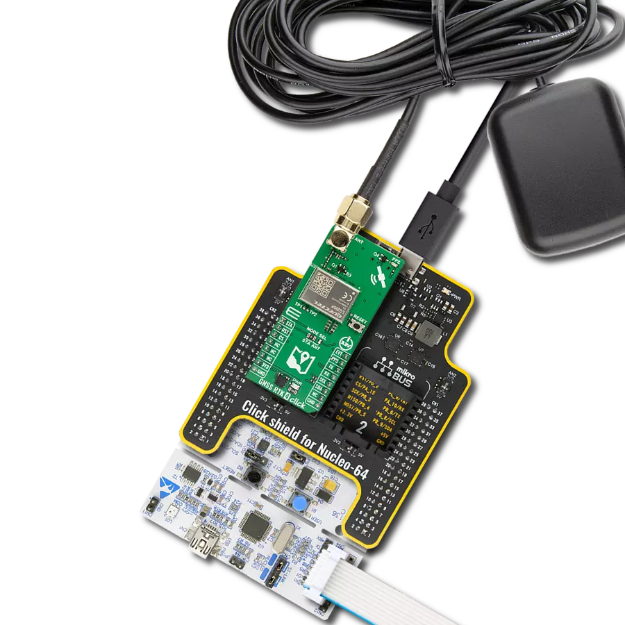
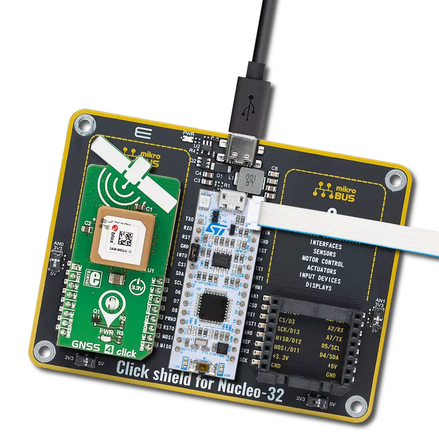
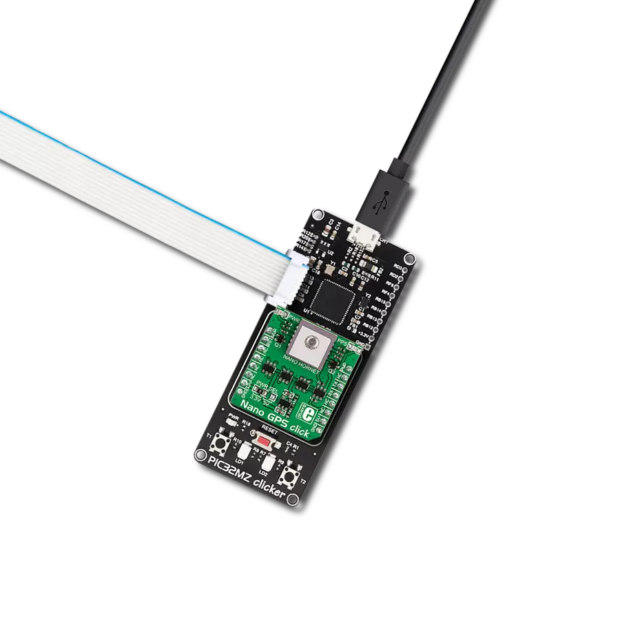
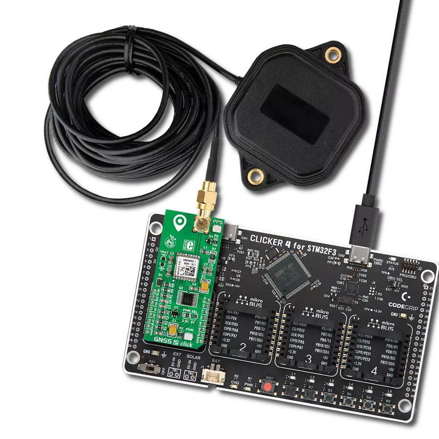
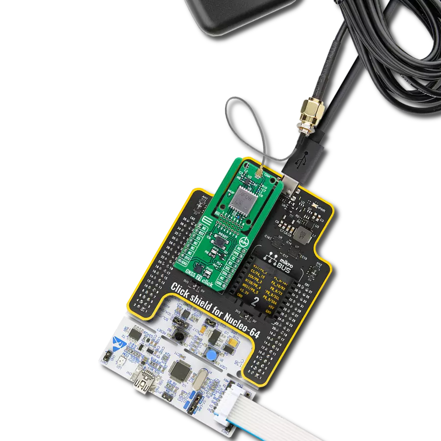
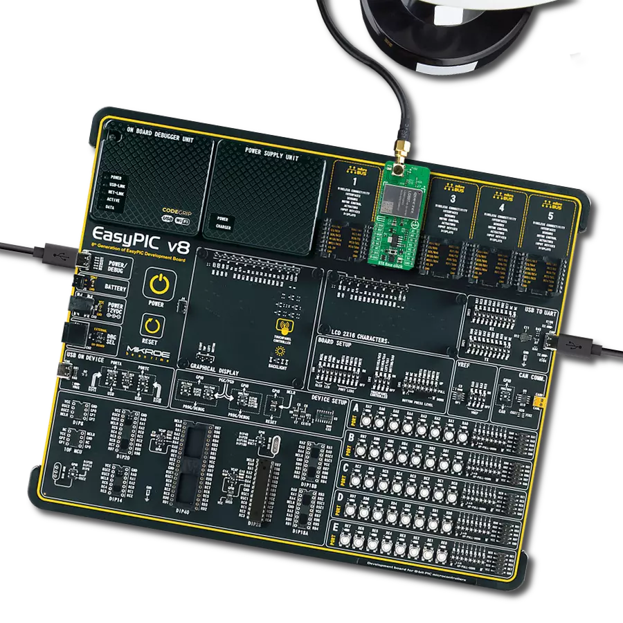
Start by selecting your development board and Click board™. Begin with the Arduino UNO Rev3 as your development board.


Software Support
Library Description
This library contains API for RTK Base Click driver.
Key functions:
rtkbase_generic_readThis function reads a desired number of data bytes by using UART serial interface.rtkbase_rx_bytes_availableThis function returns the number of bytes available in the RX ring buffer.rtkbase_calculate_crc24This function calculates and returns the CRC 24-bit of RTCM3 packet input. The CRC across the whole packet should sum to zero (remainder).
Open Source
Code example
The complete application code and a ready-to-use project are available through the NECTO Studio Package Manager for direct installation in the NECTO Studio. The application code can also be found on the MIKROE GitHub account.
/*!
 * @file main.c
 * @brief RTK Base Click Example.
 *
 * # Description
 * This example demonstrates the use of RTK Base Click by reading and displaying the RTCM3 messages.
 *
 * The demo application is composed of two sections :
 *
 * ## Application Init
 * Initializes the driver and logger.
 *
 * ## Application Task
 * Reads and parses the RTCM3 messages received from the module, and displays them on the USB UART.
 *
 * ## Additional Function
 * - static void rtkbase_clear_app_buf ( void )
 * - static err_t rtkbase_process_rtcm3 ( rtkbase_t *ctx )
 *
 * @note
 * The Click board comes with the default baud rate of 460800, but the baud rate is set to 115200
 * in the example due to code portability and speed limitations of some MCUs. So in order to run
 * the example you will need to adjust the baud rate using Quectel QGNSS evaluation software.
 *
 * @author Stefan Filipovic
 *
 */

#include "board.h"
#include "log.h"
#include "rtkbase.h"

#define PROCESS_BUFFER_SIZE 300

static rtkbase_t rtkbase;
static log_t logger;

static char app_buf[ PROCESS_BUFFER_SIZE ] = { 0 };
static uint16_t app_buf_len = 0;

/**
 * @brief RTK Base clearing application buffer.
 * @details This function clears memory of application buffer and reset its length.
 * @return None.
 * @note None.
 */
static void rtkbase_clear_app_buf ( void );

/**
 * @brief RTK Base process rtcm3 function.
 * @details This function reads and processes the RTCM3 messages and displays them on the USB UART.
 * @param[in] ctx : Click context object.
 * See #rtkbase_t object definition for detailed explanation.
 * @return @li @c  0 - Successfully read RTCM3 message.
 *         @li @c -1 - Read error.
 * See #err_t definition for detailed explanation.
 * @note None.
 */
static err_t rtkbase_process_rtcm3 ( rtkbase_t *ctx );

void application_init ( void )
{
    log_cfg_t log_cfg;  /**< Logger config object. */
    rtkbase_cfg_t rtkbase_cfg;  /**< Click config object. */

    /**
     * Logger initialization.
     * Default baud rate: 115200
     * Default log level: LOG_LEVEL_DEBUG
     * @note If USB_UART_RX and USB_UART_TX
     * are defined as HAL_PIN_NC, you will
     * need to define them manually for log to work.
     * See @b LOG_MAP_USB_UART macro definition for detailed explanation.
     */
    LOG_MAP_USB_UART( log_cfg );
    log_init( &logger, &log_cfg );
    log_info( &logger, " Application Init " );

    // Click initialization.
    rtkbase_cfg_setup( &rtkbase_cfg );
    RTKBASE_MAP_MIKROBUS( rtkbase_cfg, MIKROBUS_1 );
    if ( UART_ERROR == rtkbase_init( &rtkbase, &rtkbase_cfg ) )
    {
        log_error( &logger, " Communication init." );
        for ( ; ; );
    }
    log_info( &logger, " Application Task " );
}

void application_task ( void )
{
    rtkbase_process_rtcm3 ( &rtkbase );
    rtkbase_clear_app_buf( );
}

int main ( void )
{
    /* Do not remove this line or clock might not be set correctly. */
    #ifdef PREINIT_SUPPORTED
    preinit();
    #endif

    application_init( );

    for ( ; ; )
    {
        application_task( );
    }

    return 0;
}

static void rtkbase_clear_app_buf ( void )
{
    memset( app_buf, 0, app_buf_len );
    app_buf_len = 0;
}

static err_t rtkbase_process_rtcm3 ( rtkbase_t *ctx )
{
    #define RTKBASE_HEADER_0    0xD3
    #define RTKBASE_HEADER_1    0x00
    for ( ; ; ) // loop until a header byte 0 is read
    {
        while ( rtkbase_rx_bytes_available ( ctx ) < 1 );

        if ( 1 == rtkbase_generic_read( ctx, app_buf, 1 ) )
        {
            if ( RTKBASE_HEADER_0 == app_buf[ 0 ] )
            {
                break;
            }
        }
    }
    // wait until a header byte 1 and packet size bytes are available for read
    while ( rtkbase_rx_bytes_available ( ctx ) < 2 );
    if ( 2 != rtkbase_generic_read( ctx, &app_buf[ 1 ], 2 ) )
    {
        return RTKBASE_ERROR;
    }
    if ( RTKBASE_HEADER_1 != ( app_buf[ 1 ] & 0xFC ) )
    {
        return RTKBASE_ERROR;
    }
    app_buf_len = ( ( uint16_t ) ( app_buf[ 1 ] & 0x03 ) << 8 ) + app_buf[ 2 ] + 6; // Header + size + payload bytes + CRC bytes

    // wait until payload and CRC bytes are available for read
    while ( rtkbase_rx_bytes_available ( ctx ) < ( app_buf_len - 3 ) );
    if ( ( app_buf_len - 3 ) != rtkbase_generic_read( ctx, &app_buf[ 3 ], ( app_buf_len - 3 ) ) )
    {
        return RTKBASE_ERROR;
    }

    // The CRC across the whole packet should sum to zero (remainder)
    if ( 0 == rtkbase_calculate_crc24( app_buf, app_buf_len ) )
    {
        uint16_t rtcm3_msg_type = ( ( uint16_t ) app_buf[ 3 ] << 4 ) | ( ( app_buf[ 4 ] >> 4 ) & 0x0F ); // 12-bit message type
        log_printf ( &logger, "\r\n\n RTCM3 -> Type: %u; Size: %u;\r\n", rtcm3_msg_type, app_buf_len );
        for ( int32_t cnt = 0; cnt < app_buf_len; cnt++ )
        {
            log_printf( &logger, " %.2X", ( uint16_t ) app_buf[ cnt ] );
            if ( ( cnt % 16 ) == 15 )
            {
                log_printf( &logger, "\r\n" );
            }
        }
        return RTKBASE_OK;
    }
    return RTKBASE_ERROR;
}

// ------------------------------------------------------------------------ END
Additional Support
Resources
Category:GPS/GNSS