Convert real-world physical quantities into digital data with AD7124-8 and STM32F303VC
Eight-channel isolated sigma-delta ADC with PGA

Published Feb 14, 2024
Click board™
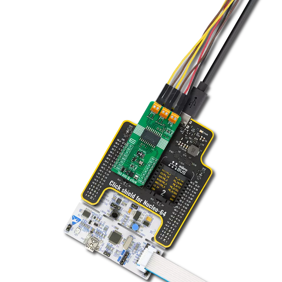
ISO ADC 6 Click
Dev. board
Discovery kit with STM32F303VC MCU
Compiler
NECTO Studio
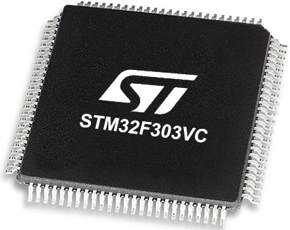
MCU
STM32F303VC
High-precision analog-to-digital conversion with isolation capabilities suitable for various industrial and measurement applications
A
A
Hardware Overview
How does it work?
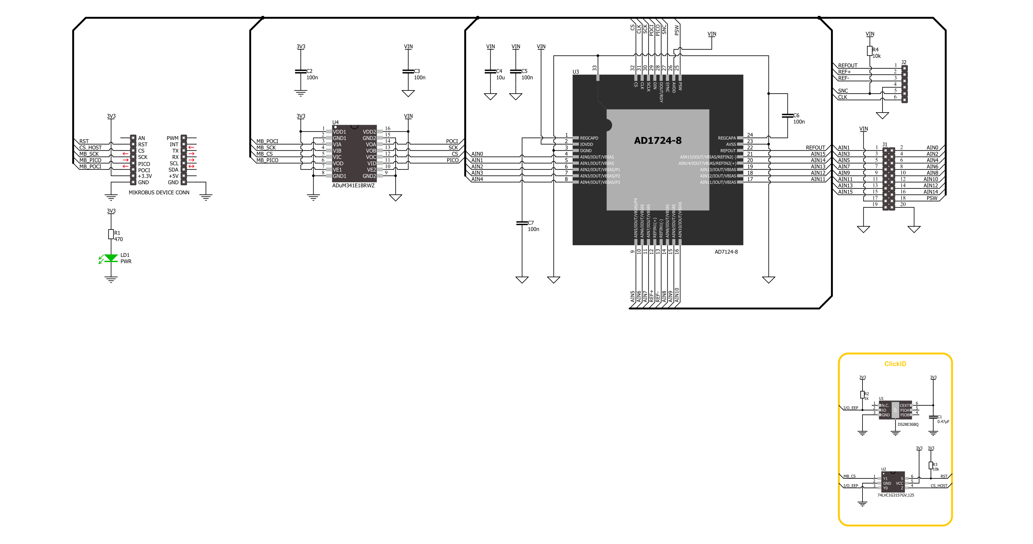
ISO ADC 6 Click is based on the AD7124-8, an 8-channel, low noise, low power, 24-bit, sigma-delta ADC, and the ADuM341E, a 5kVrms quad digital isolator, both from Analog Devices. The ADC incorporates a sigma-delta modulator, buffer, reference, gain stage, and on-chip digital filtering. It is intended to measure wide dynamic ranges, weigh scales, temperature measurement applications, and low-frequency signals. The ADC allows up to 16 configurations or channels consisting of analog inputs, reference inputs, or power supplies. All ADC channels are available over the A0-15 header, with a common GND, power supply, and a bridge power switch (PSW). You can add an external reference over the REF+ and REF-
pins. The internal reference has its output available over the REFOUT pin. The synchronization input is also available over the SNC pin. It allows synchronization of the digital filters and analog modulators when using several AD7124-8 devices. For this purpose, the internal clock is available over the CLK pin. Alternatively, the internal clock can be turned off, and this pin can provide an external clock, allowing simultaneous conversions. The isolator isolates the ADC communication lines to the host MCU. It features low propagation delay, low dynamic power consumption, 100Mbps maximum guaranteed data rate, and more. The isolator is based on CMOS, a monolithic air core transformer technology, and iCoupler technology.
ISO ADC 6 Click uses a standard 4-wire SPI serial interface of the ADC to communicate with the host MCU over the isolator barrier. The isolator uses a high-frequency carrier to transmit data across the isolation barrier using iCoupler chip scale transformer coils separated by layers of polyimide isolation. The ADC can work in three power modes, which allows sampling in a range of 1.17sps up to 19200sps. This Click board™ can be operated only with a 3.3V logic voltage level. The board must perform appropriate logic voltage level conversion before using MCUs with different logic levels. Also, it comes equipped with a library containing functions and an example code that can be used as a reference for further development.

Features overview
Development board
Discovery kit with STM32F303VC MCU streamlines application development with the STM32F3 Series microcontroller, harnessing the robustness of Arm® Cortex®-M4 architecture to provide an optimal development experience. It caters to both beginners and experts, offering essential components for swift initiation. Powered by the STM32F303VCT6, it boasts features like ST-
LINK/V2 or ST-LINK/V2-B for debugging, accelerometer, gyroscope, e-compass ST MEMS, USB connectivity, LED indicators, and push-buttons. Key specifications include a 256-Kbyte Flash memory, 48-Kbyte RAM, USB FS support, and a comprehensive array of motion sensors. The board includes ten LEDs for various statuses, including power indication and USB
communication. With user-friendly connectors and flexible power-supply options, it enables easy integration with prototype boards. Equipped with an on-board debugger/programmer and support for various Integrated Development Environments (IDEs) like IAR™, Keil®, and STM32CubeIDE, it ensures smooth and efficient development cycles.

Microcontroller Overview
MCU Card / MCU
Architecture
ARM Cortex-M4
MCU Memory (KB)
256
Silicon Vendor
STMicroelectronics
Pin count
100
RAM (Bytes)
40960
You complete me!
Accessories
STM32F3 Discovery Shield is the perfect extension for your STM32F3 Discovery Board from STMicroelectronics. This versatile shield features four mikroBUS™ host sockets, a USB-UART module, and a CAN transceiver, expanding the capabilities of your Discovery board. Acting as a docking station, the STM32F3 Discovery Shield enables you to effortlessly transform your board into various applications, whether it's an RFID lock, SMS-triggered control switch, GPS tracking device, full-blown weather station, or any other idea you have in mind. With its seamless integration and enhanced functionality, this shield empowers you to explore endless possibilities and quickly bring your projects to life.

Used MCU Pins
mikroBUS™ mapper
Take a closer look
Click board™ Schematic
Step by step
Project assembly

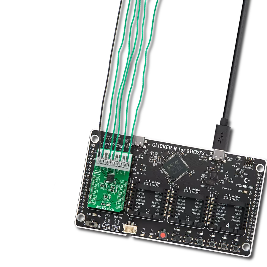
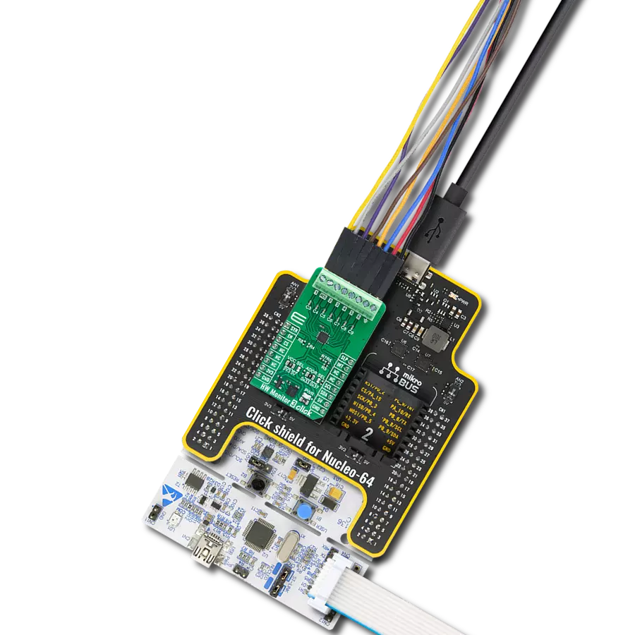
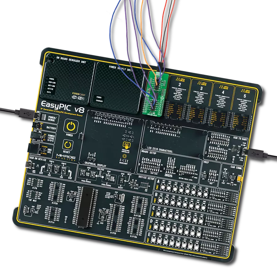
Start by selecting your development board and Click board™. Begin with the Discovery kit with STM32F303VC MCU as your development board.


Track your results in real time
Application Output
1. Application Output - In Debug mode, the 'Application Output' window enables real-time data monitoring, offering direct insight into execution results. Ensure proper data display by configuring the environment correctly using the provided tutorial.

2. UART Terminal - Use the UART Terminal to monitor data transmission via a USB to UART converter, allowing direct communication between the Click board™ and your development system. Configure the baud rate and other serial settings according to your project's requirements to ensure proper functionality. For step-by-step setup instructions, refer to the provided tutorial.

3. Plot Output - The Plot feature offers a powerful way to visualize real-time sensor data, enabling trend analysis, debugging, and comparison of multiple data points. To set it up correctly, follow the provided tutorial, which includes a step-by-step example of using the Plot feature to display Click board™ readings. To use the Plot feature in your code, use the function: plot(*insert_graph_name*, variable_name);. This is a general format, and it is up to the user to replace 'insert_graph_name' with the actual graph name and 'variable_name' with the parameter to be displayed.

Software Support
Library Description
This library contains API for ISO ADC 6 Click driver.
Key functions:
isoadc6_get_voltage- ISO ADC 6 get voltage level functionisoadc6_get_adc_data- ISO ADC 6 get ADC data functionisoadc6_set_adc_control- ISO ADC 6 set ADC control function
Open Source
Code example
The complete application code and a ready-to-use project are available through the NECTO Studio Package Manager for direct installation in the NECTO Studio. The application code can also be found on the MIKROE GitHub account.
/*!
 * @file main.c
 * @brief ISO ADC 6 Click example
 *
 * # Description
 * This example demonstrates the use of the ISO ADC 6 Click board™
 * by reading and writing data by using SPI serial interface
 * and reading results of AD conversion.
 *
 * The demo application is composed of two sections :
 *
 * ## Application Init
 * Initialization of SPI module and log UART.
 * After driver initialization, the app executes a default configuration which enables channel 0,
 * puts A0 on positive analog input and A1 on negative analog input,
 * enables internal reference voltage (approximately 2.65V (AVDD = 3.3V)),
 * and also enables bipolar operation mode and puts device on full power mode.
 *
 * ## Application Task
 * The demo application reads the voltage levels from analog input (A0-A1) and displays the results.
 * Results are being sent to the UART Terminal, where you can track their changes.
 *
 * @author Mikroe Team
 *
 */

#include "board.h"
#include "log.h"
#include "isoadc6.h"

static isoadc6_t isoadc6;
static log_t logger;

void application_init ( void )
{
    log_cfg_t log_cfg;  /**< Logger config object. */
    isoadc6_cfg_t isoadc6_cfg;  /**< Click config object. */

    /**
     * Logger initialization.
     * Default baud rate: 115200
     * Default log level: LOG_LEVEL_DEBUG
     * @note If USB_UART_RX and USB_UART_TX
     * are defined as HAL_PIN_NC, you will
     * need to define them manually for log to work.
     * See @b LOG_MAP_USB_UART macro definition for detailed explanation.
     */
    LOG_MAP_USB_UART( log_cfg );
    log_init( &logger, &log_cfg );
    log_info( &logger, " Application Init " );

    // Click initialization.
    isoadc6_cfg_setup( &isoadc6_cfg );
    ISOADC6_MAP_MIKROBUS( isoadc6_cfg, MIKROBUS_1 );
    if ( SPI_MASTER_ERROR == isoadc6_init( &isoadc6, &isoadc6_cfg ) )
    {
        log_error( &logger, " Communication init." );
        for ( ; ; );
    }

    if ( ISOADC6_ERROR == isoadc6_default_cfg ( &isoadc6 ) )
    {
        log_error( &logger, " Default configuration." );
        for ( ; ; );
    }

    log_info( &logger, " Application Task " );
}

void application_task ( void )
{
    float voltage = 0;
    if ( ISOADC6_OK == isoadc6_get_voltage( &isoadc6, &voltage ) )
    {
        log_printf( &logger, " Voltage: %.3f [V]\r\n", voltage );
        Delay_ms ( 1000 );
    }
}

int main ( void )
{
    /* Do not remove this line or clock might not be set correctly. */
    #ifdef PREINIT_SUPPORTED
    preinit();
    #endif

    application_init( );

    for ( ; ; )
    {
        application_task( );
    }

    return 0;
}

// ------------------------------------------------------------------------ END