Monitor multiple voltage levels with high accuracy using the TPS389006 and STM32G474RE
Six-channel window voltage supervisor

Published Dec 04, 2024
Click board™
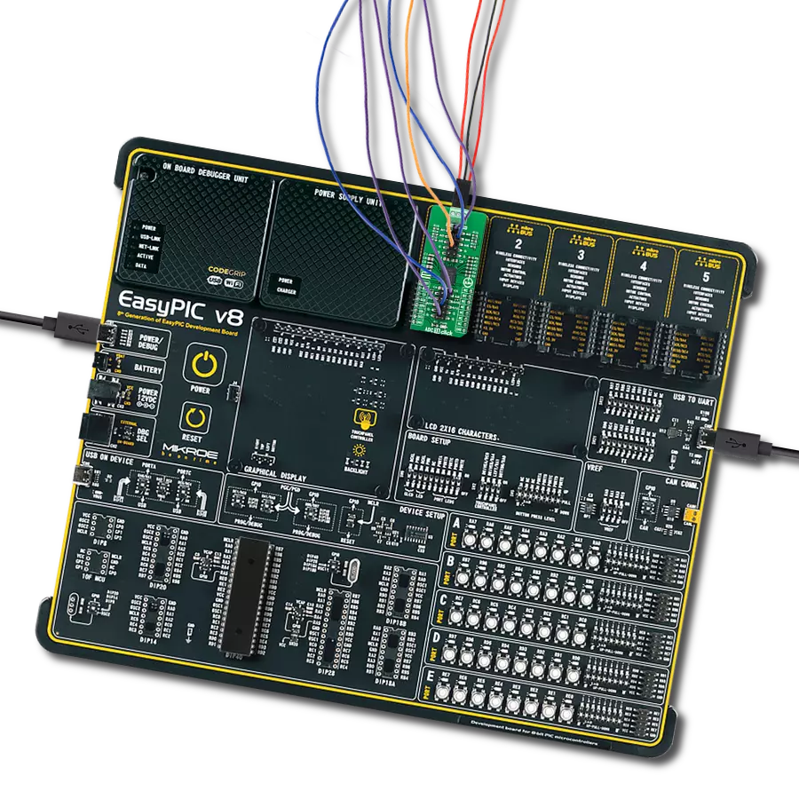
HW Monitor 3 Click
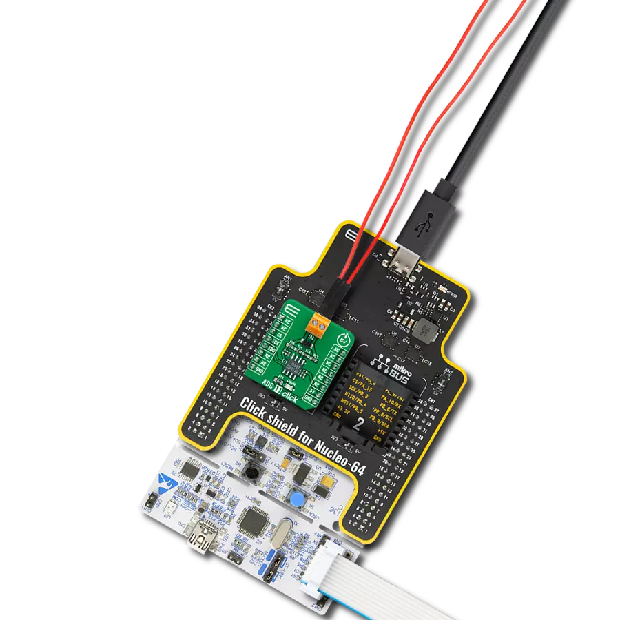
Dev. board
Nucleo 64 with STM32G474RE MCU
Compiler
NECTO Studio
MCU
STM32G474RE
Voltage monitoring with SIL-3 safety compliance perfect for medical devices, industrial robotics, and motor drivers
A
A
Hardware Overview
How does it work?
HW Monitor 3 Click is based on the TPS389006, a six-channel window voltage supervisor and monitor IC from Texas Instruments. This I2C-programmable device is engineered to provide precision voltage monitoring for systems operating on low-voltage supply rails with tight tolerance margins. The IC's thresholds for overvoltage and undervoltage conditions are internally set using precision resistors, providing ±6mV accuracy across a wide temperature range (-40°C to +125°C). It supports voltage levels with fixed window thresholds in fine steps, offering 5mV granularity for inputs between 0.2V and 1.475V or 20mV steps for higher ranges from 0.8V to 5.5V. The device also incorporates a 2.48V undervoltage lockout (UVLO) feature, ensuring stable operation in critical conditions. With compliance with SIL-3 safety standards, this board is tailored for applications requiring the highest reliability and safety, such as medical devices, industrial robotics, server switches, and motor drivers. The TPS389006 offers exceptional performance with integrated features for robust error detection and monitoring. It includes two remote sense pins for voltage measurement at
high-current core rails, compensating for voltage drops across PCB traces. This ensures highly accurate monitoring, making it ideal for systems demanding precise power management. The built-in CRC error checking and sequence logging capabilities track system states during power-up and power-down events, while an integrated ADC provides real-time voltage readouts for additional redundancy in error checking. HW Monitor 3 Click uses a standard 2-wire I2C communication protocol to enable the host MCU to control the TPS389006. The I2C interface supports clock frequencies up to 1MHz, with the I2C address selectable via the ADDR SEL jumper. The I2C interface gives flexibility in selecting thresholds, reset delays, glitch filters, and pin functionality. The internal glitch immunity and noise filters eliminate the need for external RC components to reduce false resets resulting from power transients. In addition to the interface pins, this board uses several pins from the mikroBUS™ socket to enhance its functionality. The EN pin serves as a device-enable signal, allowing activation of the TPS389006 when needed. The INT pin is an active-low open-drain
interrupt output, which asserts a signal whenever the monitored voltage moves outside the predefined safe window, providing real-time alerts for critical voltage deviations. Additionally, the SLP pin enables a low-power sleep mode through an active-low signal, optimizing power efficiency when the device is not actively monitoring. In addition, the TPS389006 offers a sync feature via the SYN pin of the mikroBUS™ socket (sequence logging synchronization across multiple devices) for tagging rails as they come up. When either the EN or SLP pin transitions from low to high or high to low, the sequence logging function becomes active until the sequence timeout expires. This Click board™ can operate with either 3.3V or 5V logic voltage levels selected via the VCC SEL jumper. This way, both 3.3V and 5V capable MCUs can use the communication lines properly. Also, this Click board™ comes equipped with a library containing easy-to-use functions and an example code that can be used as a reference for further development.

Features overview
Development board
Nucleo-64 with STM32G474R MCU offers a cost-effective and adaptable platform for developers to explore new ideas and prototype their designs. This board harnesses the versatility of the STM32 microcontroller, enabling users to select the optimal balance of performance and power consumption for their projects. It accommodates the STM32 microcontroller in the LQFP64 package and includes essential components such as a user LED, which doubles as an ARDUINO® signal, alongside user and reset push-buttons, and a 32.768kHz crystal oscillator for precise timing operations. Designed with expansion and flexibility in mind, the Nucleo-64 board features an ARDUINO® Uno V3 expansion connector and ST morpho extension pin
headers, granting complete access to the STM32's I/Os for comprehensive project integration. Power supply options are adaptable, supporting ST-LINK USB VBUS or external power sources, ensuring adaptability in various development environments. The board also has an on-board ST-LINK debugger/programmer with USB re-enumeration capability, simplifying the programming and debugging process. Moreover, the board is designed to simplify advanced development with its external SMPS for efficient Vcore logic supply, support for USB Device full speed or USB SNK/UFP full speed, and built-in cryptographic features, enhancing both the power efficiency and security of projects. Additional connectivity is
provided through dedicated connectors for external SMPS experimentation, a USB connector for the ST-LINK, and a MIPI® debug connector, expanding the possibilities for hardware interfacing and experimentation. Developers will find extensive support through comprehensive free software libraries and examples, courtesy of the STM32Cube MCU Package. This, combined with compatibility with a wide array of Integrated Development Environments (IDEs), including IAR Embedded Workbench®, MDK-ARM, and STM32CubeIDE, ensures a smooth and efficient development experience, allowing users to fully leverage the capabilities of the Nucleo-64 board in their projects.

Microcontroller Overview
MCU Card / MCU
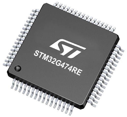
Architecture
ARM Cortex-M4
MCU Memory (KB)
512
Silicon Vendor
STMicroelectronics
Pin count
64
RAM (Bytes)
128k
You complete me!
Accessories
Click Shield for Nucleo-64 comes equipped with two proprietary mikroBUS™ sockets, allowing all the Click board™ devices to be interfaced with the STM32 Nucleo-64 board with no effort. This way, Mikroe allows its users to add any functionality from our ever-growing range of Click boards™, such as WiFi, GSM, GPS, Bluetooth, ZigBee, environmental sensors, LEDs, speech recognition, motor control, movement sensors, and many more. More than 1537 Click boards™, which can be stacked and integrated, are at your disposal. The STM32 Nucleo-64 boards are based on the microcontrollers in 64-pin packages, a 32-bit MCU with an ARM Cortex M4 processor operating at 84MHz, 512Kb Flash, and 96KB SRAM, divided into two regions where the top section represents the ST-Link/V2 debugger and programmer while the bottom section of the board is an actual development board. These boards are controlled and powered conveniently through a USB connection to program and efficiently debug the Nucleo-64 board out of the box, with an additional USB cable connected to the USB mini port on the board. Most of the STM32 microcontroller pins are brought to the IO pins on the left and right edge of the board, which are then connected to two existing mikroBUS™ sockets. This Click Shield also has several switches that perform functions such as selecting the logic levels of analog signals on mikroBUS™ sockets and selecting logic voltage levels of the mikroBUS™ sockets themselves. Besides, the user is offered the possibility of using any Click board™ with the help of existing bidirectional level-shifting voltage translators, regardless of whether the Click board™ operates at a 3.3V or 5V logic voltage level. Once you connect the STM32 Nucleo-64 board with our Click Shield for Nucleo-64, you can access hundreds of Click boards™, working with 3.3V or 5V logic voltage levels.

Used MCU Pins
mikroBUS™ mapper
Take a closer look
Click board™ Schematic

Step by step
Project assembly
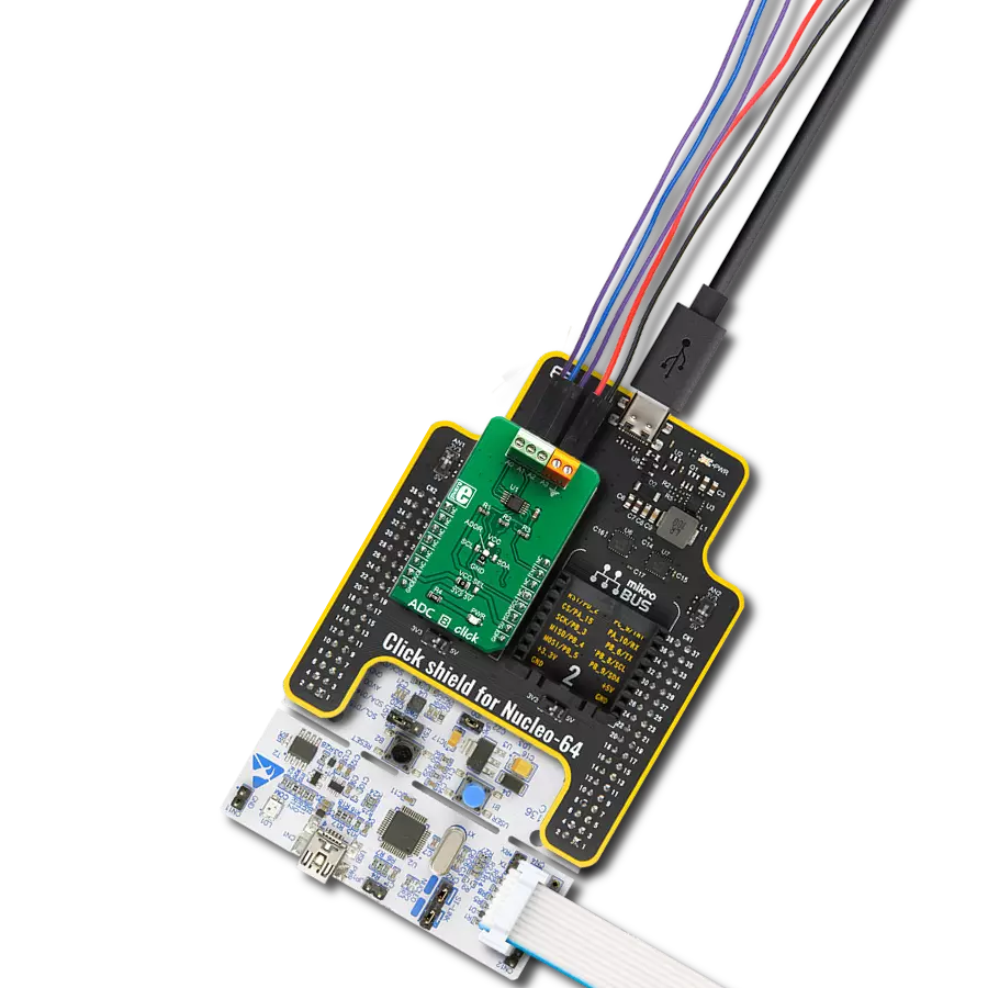
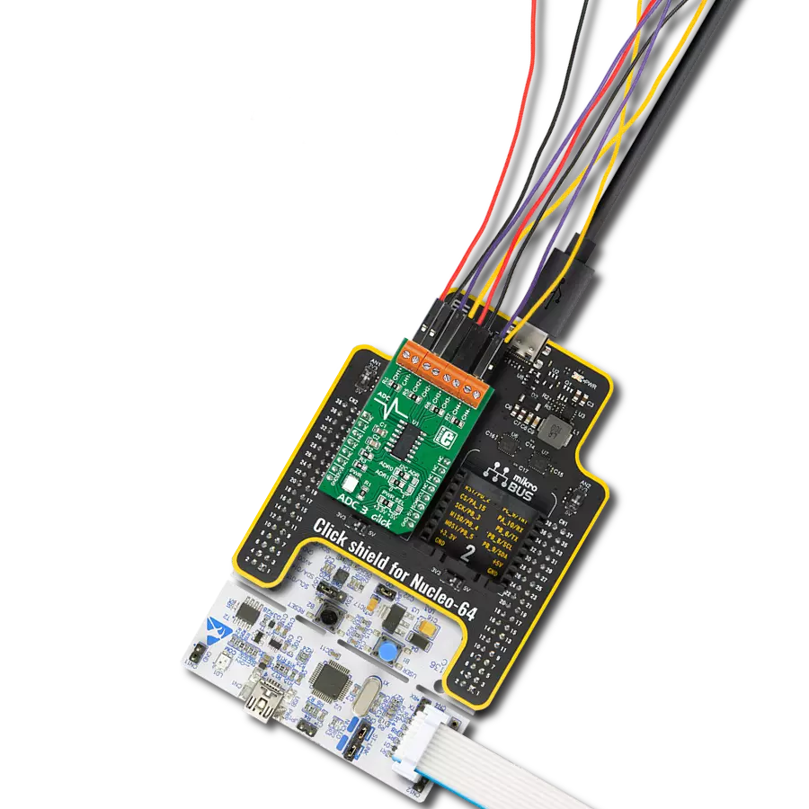
Start by selecting your development board and Click board™. Begin with the Nucleo 64 with STM32G474RE MCU as your development board.


Track your results in real time
Application Output
1. Application Output - In Debug mode, the 'Application Output' window enables real-time data monitoring, offering direct insight into execution results. Ensure proper data display by configuring the environment correctly using the provided tutorial.

2. UART Terminal - Use the UART Terminal to monitor data transmission via a USB to UART converter, allowing direct communication between the Click board™ and your development system. Configure the baud rate and other serial settings according to your project's requirements to ensure proper functionality. For step-by-step setup instructions, refer to the provided tutorial.

3. Plot Output - The Plot feature offers a powerful way to visualize real-time sensor data, enabling trend analysis, debugging, and comparison of multiple data points. To set it up correctly, follow the provided tutorial, which includes a step-by-step example of using the Plot feature to display Click board™ readings. To use the Plot feature in your code, use the function: plot(*insert_graph_name*, variable_name);. This is a general format, and it is up to the user to replace 'insert_graph_name' with the actual graph name and 'variable_name' with the parameter to be displayed.

Software Support
Library Description
This library contains API for HW Monitor 3 Click driver.
Key functions:
hwmonitor3_enable_channel- This function enables the selected monitoring channels.hwmonitor3_set_scaling- This function sets the scaling level for the selected monitoring channels.hwmonitor3_read_voltage- This function reads the voltage level from all 6 monitoring analog input channels.
Open Source
Code example
The complete application code and a ready-to-use project are available through the NECTO Studio Package Manager for direct installation in the NECTO Studio. The application code can also be found on the MIKROE GitHub account.
/*!
 * @file main.c
 * @brief HW Monitor 3 Click example
 *
 * # Description
 * This example demonstrates the use of HW Monitor 3 Click board by reading and
 * displaying the voltage level from 6 analog input channels.
 *
 * The demo application is composed of two sections :
 *
 * ## Application Init
 * Initializes the driver and performs the Click default configuration.
 *
 * ## Application Task
 * Reads the voltage level from all 6 analog input channels and displays
 * the results on the USB UART once per second approximately.
 *
 * @author Stefan Filipovic
 *
 */

#include "board.h"
#include "log.h"
#include "hwmonitor3.h"

static hwmonitor3_t hwmonitor3;
static log_t logger;

void application_init ( void )
{
    log_cfg_t log_cfg;  /**< Logger config object. */
    hwmonitor3_cfg_t hwmonitor3_cfg;  /**< Click config object. */

    /**
     * Logger initialization.
     * Default baud rate: 115200
     * Default log level: LOG_LEVEL_DEBUG
     * @note If USB_UART_RX and USB_UART_TX
     * are defined as HAL_PIN_NC, you will
     * need to define them manually for log to work.
     * See @b LOG_MAP_USB_UART macro definition for detailed explanation.
     */
    LOG_MAP_USB_UART( log_cfg );
    log_init( &logger, &log_cfg );
    log_info( &logger, " Application Init " );

    // Click initialization.
    hwmonitor3_cfg_setup( &hwmonitor3_cfg );
    HWMONITOR3_MAP_MIKROBUS( hwmonitor3_cfg, MIKROBUS_1 );
    if ( I2C_MASTER_ERROR == hwmonitor3_init( &hwmonitor3, &hwmonitor3_cfg ) )
    {
        log_error( &logger, " Communication init." );
        for ( ; ; );
    }

    if ( HWMONITOR3_ERROR == hwmonitor3_default_cfg ( &hwmonitor3 ) )
    {
        log_error( &logger, " Default configuration." );
        for ( ; ; );
    }

    log_info( &logger, " Application Task " );
}

void application_task ( void )
{
    hwmonitor3_ch_mon_t ch_mon;
    if ( HWMONITOR3_OK == hwmonitor3_read_voltage ( &hwmonitor3, &ch_mon ) )
    {
        log_printf ( &logger, " CH1: %.3f V\r\n", ch_mon.ch1_v );
        log_printf ( &logger, " CH2: %.3f V\r\n", ch_mon.ch2_v );
        log_printf ( &logger, " CH3: %.3f V\r\n", ch_mon.ch3_v );
        log_printf ( &logger, " CH4: %.3f V\r\n", ch_mon.ch4_v );
        log_printf ( &logger, " CH5: %.3f V\r\n", ch_mon.ch5_v );
        log_printf ( &logger, " CH6: %.3f V\r\n\n", ch_mon.ch6_v );
    }
    Delay_ms ( 1000 );
}

int main ( void )
{
    /* Do not remove this line or clock might not be set correctly. */
    #ifdef PREINIT_SUPPORTED
    preinit();
    #endif

    application_init( );

    for ( ; ; )
    {
        application_task( );
    }

    return 0;
}

// ------------------------------------------------------------------------ END
Additional Support
Resources
Category:ADC