Switch between various analog inputs dynamically with ADG1438 and STM32F407VGT6
Unveil possibilities with analog multiplexing

Published Feb 14, 2024
Click board™
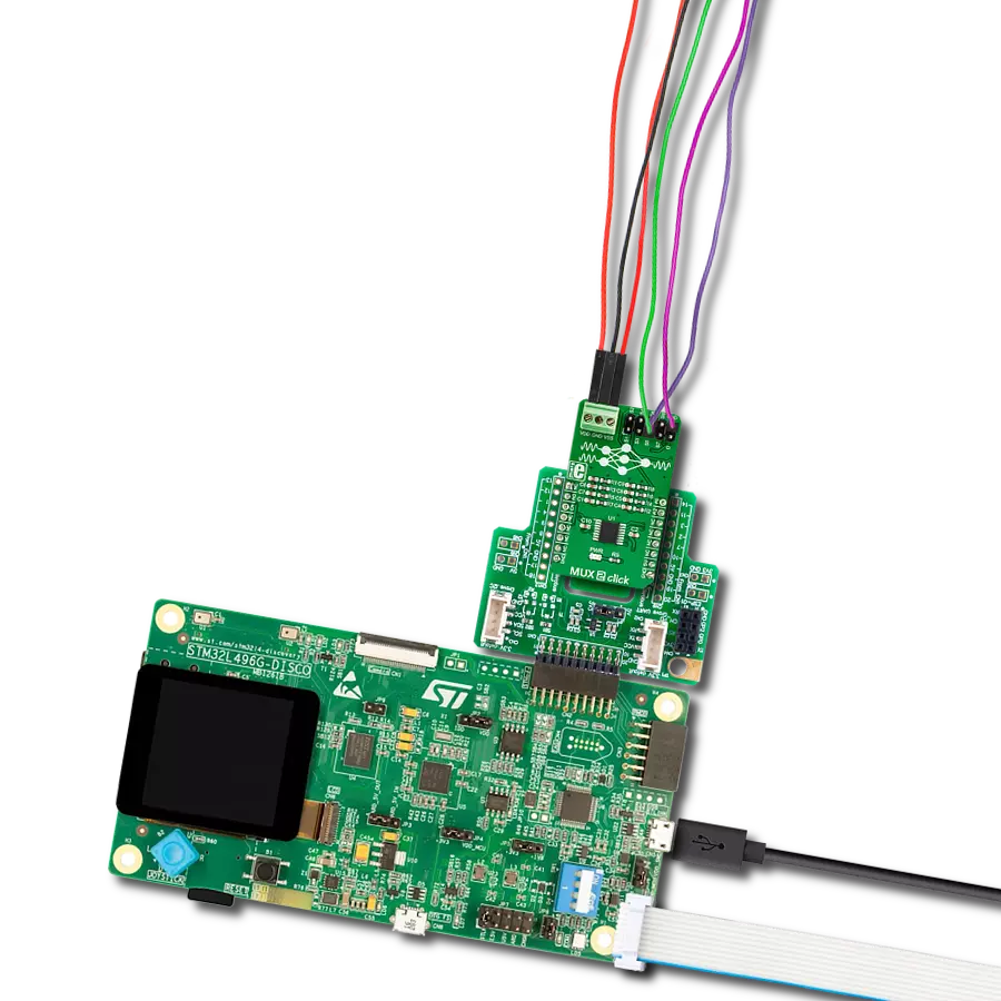
MUX 9 Click
Dev. board
Discovery kit with STM32F407VG MCU
Compiler
NECTO Studio
MCU
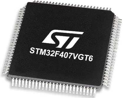
STM32F407VGT6
Optimize resource utilization, and enable several analog inputs to be efficiently combined and transmitted, saving space, energy, and resources
A
A
Hardware Overview
How does it work?
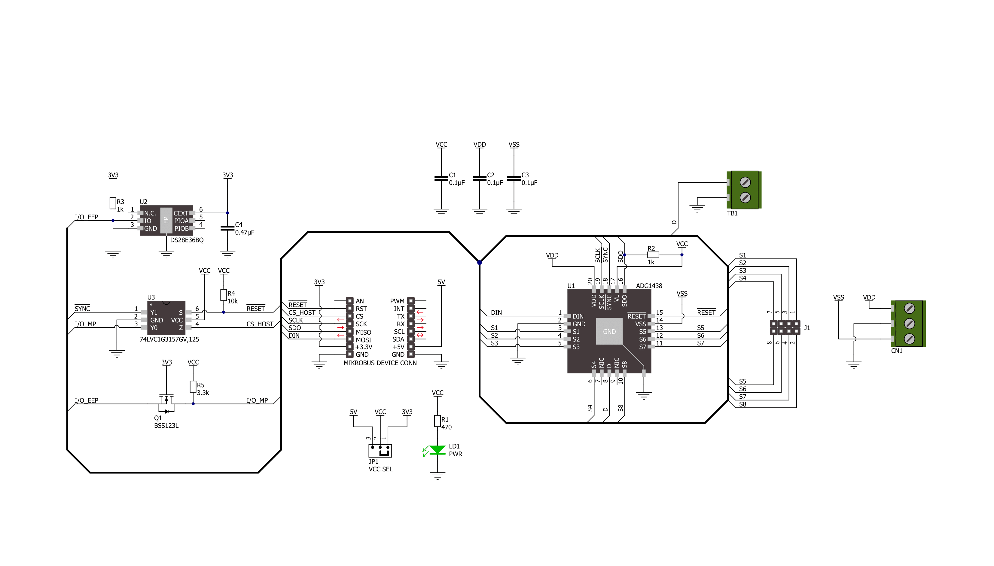
MUX 9 Click is based on the ADG1438, a serially controlled, 8-channel analog multiplexer from Analog Devices. Each switch is software-controlled (by a bit of the appropriate register) and conducts equally well in both directions, making it ideal for standard multiplexing and demultiplexing. Because each switch is independently controlled by an individual bit, this allows having any, all, or none of the switches on (logic 1 in a particular bit position turns the switch ON, whereas Logic 0 turns the switch OFF). This feature may be handy in the demultiplexing application, where the user may wish to direct one signal from the drain terminal, marked as D, to several outputs (sources). This Click board™ communicates with the MCU
through a standard SPI interface (compatible with SPI, QSPI™, MICROWIRE™, and DSP interface standards) supporting the most common SPI mode, SPI Mode 1, with a maximum frequency of 50MHz. During the Power-Up sequence, the internal shift register contains all zeros, and all switches are in the OFF state and remain so until a valid write takes place. This state can also be achieved with the help of an active-low reset pin, controlled via the RST pin of the mikroBUS™ socket. All switches are off by setting this pin to a low logic level, and the appropriate registers are cleared to 0. As for the input signal range, it extends over the power supply rails' capacity. The ADG1438 is specified for a wide supply
range ±15V/+12V/±5V, where all channels exhibit break-before-make switching action, preventing momentary shorting when switching channels. Also, these switches' ultra-low on-resistance and on-resistance flatness make them ideal solutions for data acquisition and gain switching applications where low distortion is critical. This Click board™ can operate with either 3.3V or 5V logic voltage levels selected via the VCC SEL jumper. This way, both 3.3V and 5V capable MCUs can use the communication lines properly. Also, this Click board™ comes equipped with a library containing easy-to-use functions and an example code that can be used, as a reference, for further development.


Features overview
Development board
Discovery kit with STM32F407VG MCU, powered by the STM32F407 microcontroller, simplifies audio application development. It offers a robust platform with features like the ST-LINK/V2-A debugger, STMEMS digital accelerometer, digital microphone, and integrated audio DAC with a class D speaker driver. It has LEDs, push buttons, and a USB OTG
Micro-AB connector for versatile connectivity. The STM32F407VGT6 MCU boasts a 32-bit Arm Cortex-M4 with FPU, 1MB Flash memory, and 192KB RAM, housed in an LQFP100 package. Equipped with USB OTG FS, MEMS accelerometer, omnidirectional digital microphone, and user-friendly buttons, it ensures seamless operation.
The board accommodates various add-ons via extension headers while offering flexible power supply options, including ST-LINK, USB VBUS, or external sources. Supported by comprehensive free software and a range of IDEs, it empowers developers with flexibility and ease of use, making it an ideal choice for audio-centric projects.

Microcontroller Overview
MCU Card / MCU
Architecture
ARM Cortex-M4
MCU Memory (KB)
10
Silicon Vendor
STMicroelectronics
Pin count
100
RAM (Bytes)
100
You complete me!
Accessories
STM32F4 Discovery Shield is the perfect extension for your STM32F4 Discovery Board from STMicroelectronics. This versatile shield features four mikroBUS™ host sockets, a USB-UART module, and a CAN transceiver, expanding the capabilities of your Discovery board. Acting as a docking station, the STM32F4 Discovery Shield enables you to effortlessly transform your board into various applications, whether it's an RFID lock, SMS-triggered control switch, GPS tracking device, full-blown weather station, or any other idea you have in mind. With its seamless integration and enhanced functionality, this shield empowers you to explore endless possibilities and quickly bring your projects to life.

Used MCU Pins
mikroBUS™ mapper
Take a closer look
Click board™ Schematic
Step by step
Project assembly

Start by selecting your development board and Click board™. Begin with the Discovery kit with STM32F407VG MCU as your development board.


Track your results in real time
Application Output
1. Application Output - In Debug mode, the 'Application Output' window enables real-time data monitoring, offering direct insight into execution results. Ensure proper data display by configuring the environment correctly using the provided tutorial.

2. UART Terminal - Use the UART Terminal to monitor data transmission via a USB to UART converter, allowing direct communication between the Click board™ and your development system. Configure the baud rate and other serial settings according to your project's requirements to ensure proper functionality. For step-by-step setup instructions, refer to the provided tutorial.

3. Plot Output - The Plot feature offers a powerful way to visualize real-time sensor data, enabling trend analysis, debugging, and comparison of multiple data points. To set it up correctly, follow the provided tutorial, which includes a step-by-step example of using the Plot feature to display Click board™ readings. To use the Plot feature in your code, use the function: plot(*insert_graph_name*, variable_name);. This is a general format, and it is up to the user to replace 'insert_graph_name' with the actual graph name and 'variable_name' with the parameter to be displayed.

Software Support
Library Description
This library contains API for MUX 9 Click driver.
Key functions:
mux9_active_channel- MUX 9 active channel functionmux9_reset- MUX 9 reset functionmux9_disable- MUX 9 disable function
Open Source
Code example
The complete application code and a ready-to-use project are available through the NECTO Studio Package Manager for direct installation in the NECTO Studio. The application code can also be found on the MIKROE GitHub account.
/*!
 * @file main.c
 * @brief MUX 9 Click example
 *
 * # Description
 * This example demonstrates the use of MUX 9 Click board™.
 *
 * The demo application is composed of two sections :
 *
 * ## Application Init
 * Initializes the driver and performs the reset.
 *
 * ## Application Task
 * This is an example that shows the use of a MUX 9 Click board™.
 * This example shows switching channels (from CH 1 to CH 8) on and off.
 * Results are being sent to the Usart Terminal where you can track their changes.
 *
 * @author Nenad Filipovic
 *
 */

#include "board.h"
#include "log.h"
#include "mux9.h"

static mux9_t mux9;
static log_t logger;

void application_init ( void )
{
    log_cfg_t log_cfg;    /**< Logger config object. */
    mux9_cfg_t mux9_cfg;  /**< Click config object. */

    /**
     * Logger initialization.
     * Default baud rate: 115200
     * Default log level: LOG_LEVEL_DEBUG
     * @note If USB_UART_RX and USB_UART_TX
     * are defined as HAL_PIN_NC, you will
     * need to define them manually for log to work.
     * See @b LOG_MAP_USB_UART macro definition for detailed explanation.
     */
    LOG_MAP_USB_UART( log_cfg );
    log_init( &logger, &log_cfg );
    log_info( &logger, " Application Init " );

    // Click initialization.
    mux9_cfg_setup( &mux9_cfg );
    MUX9_MAP_MIKROBUS( mux9_cfg, MIKROBUS_1 );
    if ( SPI_MASTER_ERROR == mux9_init( &mux9, &mux9_cfg ) )
    {
        log_error( &logger, " Communication init." );
        for ( ; ; );
    }

    mux9_reset( &mux9 );
    log_info( &logger, " Application Task " );
    log_printf( &logger, " -----------\r\n" );
}

void application_task ( void )
{
    for ( uint8_t ch_pos = MUX9_SELECT_CH_1; ch_pos <= MUX9_SELECT_CH_8; ch_pos++ )
    {
        if ( MUX9_OK == mux9_active_channel( &mux9, ch_pos ) )
        {
            log_printf( &logger, " The Channel %d is activated. \r\n", ( uint16_t ) ch_pos );
            Delay_ms ( 1000 );
        }
    }
    log_printf( &logger, " -----------\r\n" );
    Delay_ms ( 1000 );
}

int main ( void )
{
    /* Do not remove this line or clock might not be set correctly. */
    #ifdef PREINIT_SUPPORTED
    preinit();
    #endif

    application_init( );

    for ( ; ; )
    {
        application_task( );
    }

    return 0;
}

// ------------------------------------------------------------------------ END