Unleash the full potential of connectivity with NINA-B1 and STM32F756ZG
Embrace wireless freedom with Bluetooth
Published Sep 17, 2024
Click board™
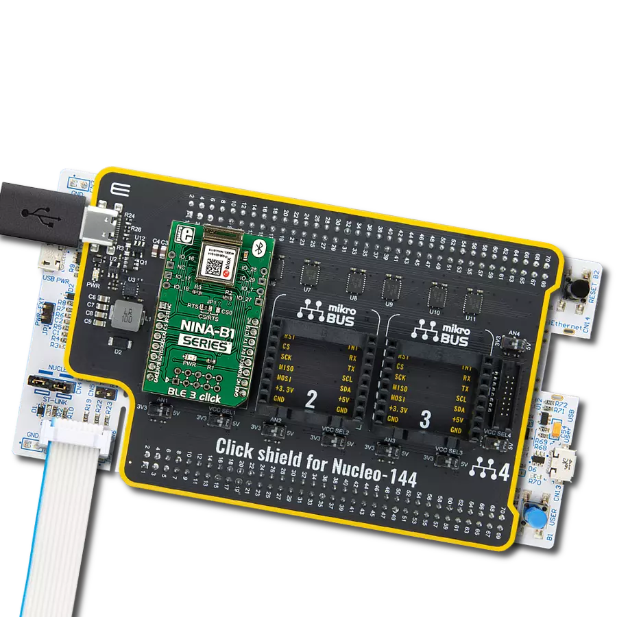
BLE 3 Click
Dev. board
Nucleo 144 with STM32F756ZG MCU
Compiler
NECTO Studio
MCU
STM32F756ZG
Take your smart solution to the next level. Integrate Bluetooth Low Energy (BLE) and soar!
A
A
Hardware Overview
How does it work?
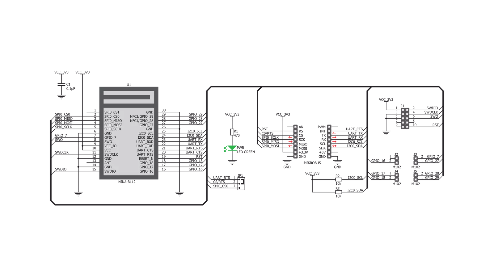
BLE 3 Click is based on the NINA-B1112-04B-04B, an open CPU stand-alone Bluetooth module from u-blox. Under the metal hood is an nRF52832, a 32-bit ARM Coretx-M4 microcontroller with FPU from Nordic Semiconductor that runs on 64MHz. It comes with 64KB RAM and 512KB flash memory and provides a rich peripheral GPIO pinout that can be used over two 4-pin headers on the sides of the module. Over those headers, the NINA-B1112-04B module exposes one general-purpose IO, 4 GPIO with analog capabilities, and two NFC pins that can be used as GPIO. Those can be used for some sensors, as the ADC on this module can sample up to 200KHz using different inputs as sample triggers in 8/10/12-bit resolutions. It is even equipped with one analog comparator. The BLE 3 module comes with an RTC, which can operate in standby mode and, in general, can be used to generate precisely timed BLE advertising events (broadcasting packets to every device around). The RTC can wake the BLE 3 Click from Sleep mode and detect the NFC field and other means. The NINA-B1112-04B module is preprogrammed with a unique 48-bit Bluetooth device address. If lost or corrupted, this same address can still be recovered from the QR code printed on the module. The module is delivered with u-connectXpress
software that supports u-blox Bluetooth low energy Serial Port Service, GATT client and server, beacons, NFC, and simultaneous peripheral and central roles. This software allows configuration over an AT command set. As mentioned, the NINA-B1112-04B includes a Near Field Communication interface capable of operating as a 13.56MHz NFC tag at a bit rate of 106Kbps. As an NFC tag, data can be read from or written to the module using an NFC reader, but it can not read other tags or initiate NFC communication. Using this feature to wake the module from deep sleep is convenient. The BLE 3 Click is not equipped with the NFC antenna; however, an external NFC antenna can be connected to the IO_28 and IO_29 pins. The nRF52832 in the NINA-B1112-04B module can be used with pre-flashed software or as an open CPU module. If so, the user can run a custom application on this module, such as Arm Mbed OS. The BLE 3 Click features the 10-pin JTAG header for this purpose. In addition, you can configure NINA-B1112-04B through u-blox S-Center toolbox software using AT commands. This software is available free of charge and can be downloaded from the u-blox website. BLE 3 Click communicates with the host MCU through the UART, SPI, and I2C interfaces. On this Click
board™, there is a CS/RTS jumper in the RTS position, thus preset for the UART interface as the interface where AT commands can control this module. Besides the standard UART RX and TX pins, you can use UART RTS and CTS hardware control flow pins (RTS labeled as CS on mikroBUS™ socket). The UART interface supports baud rates up to 1Mbps. If the choice of communication is the 4-Wire SPI Serial interface, then the jumper should be positioned on CS. The SPI interface supports serial clock frequencies up to 8MHz. The standard 2-Wire I2C interface could also be used for communication with the host MCU. It supports standard (100Kbps), fast (400Kbps), and 250Kbps transmission speeds. It is worth knowing that NINA-B1112-04B supports clock stretching, which temporarily pauses any I2C communication. The last pin is the RST pin which can be used to reset the module. This Click board™ can only be operated with a 3.3V logic voltage level. The board must perform appropriate logic voltage level conversion before using MCUs with different logic levels. However, the Click board™ comes equipped with a library containing functions and an example code that can be used, as a reference, for further development.

Features overview
Development board
Nucleo-144 with STM32F756ZG MCU board offers an accessible and adaptable avenue for users to explore new ideas and construct prototypes. It allows users to tailor their experience by selecting from a range of performance and power consumption features offered by the STM32 microcontroller. With compatible boards, the
internal or external SMPS dramatically decreases power usage in Run mode. Including the ST Zio connector, expanding ARDUINO Uno V3 connectivity, and ST morpho headers facilitate easy expansion of the Nucleo open development platform. The integrated ST-LINK debugger/programmer enhances convenience by
eliminating the need for a separate probe. Moreover, the board is accompanied by comprehensive free software libraries and examples within the STM32Cube MCU Package, further enhancing its utility and value.

Microcontroller Overview
MCU Card / MCU

Architecture
ARM Cortex-M7
MCU Memory (KB)
1024
Silicon Vendor
STMicroelectronics
Pin count
144
RAM (Bytes)
327680
You complete me!
Accessories
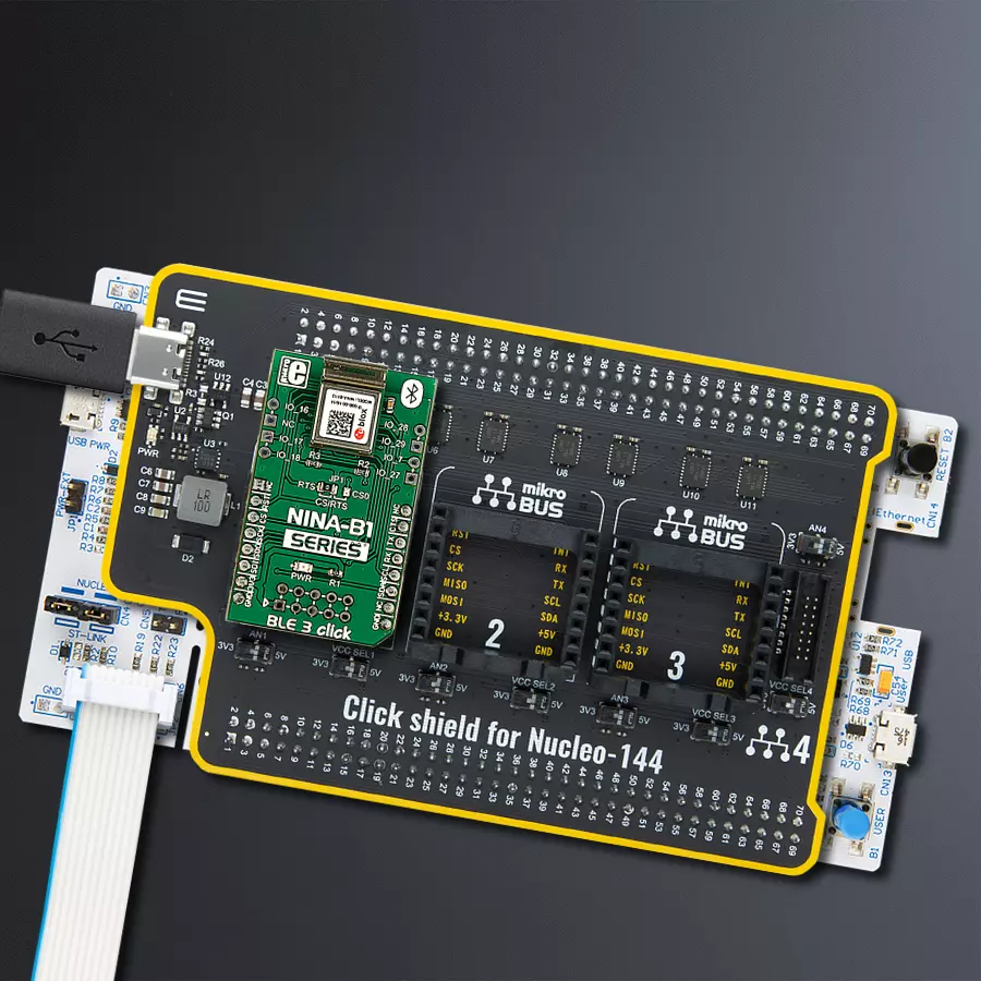
Click Shield for Nucleo-144 comes equipped with four mikroBUS™ sockets, with one in the form of a Shuttle connector, allowing all the Click board™ devices to be interfaced with the STM32 Nucleo-144 board with no effort. This way, MIKROE allows its users to add any functionality from our ever-growing range of Click boards™, such as WiFi, GSM, GPS, Bluetooth, ZigBee, environmental sensors, LEDs, speech recognition, motor control, movement sensors, and many more. Featuring an ARM Cortex-M microcontroller, 144 pins, and Arduino™ compatibility, the STM32 Nucleo-144 board offers limitless possibilities for prototyping and creating diverse applications. These boards are controlled and powered conveniently through a USB connection to program and efficiently debug the Nucleo-144 board out of the box, with an additional USB cable connected to the USB mini port on the board. Simplify your project development with the integrated ST-Link debugger and unleash creativity using the extensive I/O options and expansion capabilities. This Click Shield also has several switches that perform functions such as selecting the logic levels of analog signals on mikroBUS™ sockets and selecting logic voltage levels of the mikroBUS™ sockets themselves. Besides, the user is offered the possibility of using any Click board™ with the help of existing bidirectional level-shifting voltage translators, regardless of whether the Click board™ operates at a 3.3V or 5V logic voltage level. Once you connect the STM32 Nucleo-144 board with our Click Shield for Nucleo-144, you can access hundreds of Click boards™, working with 3.3V or 5V logic voltage levels.

Used MCU Pins
mikroBUS™ mapper
Take a closer look
Click board™ Schematic
Step by step
Project assembly
Start by selecting your development board and Click board™. Begin with the Nucleo 144 with STM32F756ZG MCU as your development board.


Track your results in real time
Application Output
1. Application Output - In Debug mode, the 'Application Output' window enables real-time data monitoring, offering direct insight into execution results. Ensure proper data display by configuring the environment correctly using the provided tutorial.

2. UART Terminal - Use the UART Terminal to monitor data transmission via a USB to UART converter, allowing direct communication between the Click board™ and your development system. Configure the baud rate and other serial settings according to your project's requirements to ensure proper functionality. For step-by-step setup instructions, refer to the provided tutorial.

3. Plot Output - The Plot feature offers a powerful way to visualize real-time sensor data, enabling trend analysis, debugging, and comparison of multiple data points. To set it up correctly, follow the provided tutorial, which includes a step-by-step example of using the Plot feature to display Click board™ readings. To use the Plot feature in your code, use the function: plot(*insert_graph_name*, variable_name);. This is a general format, and it is up to the user to replace 'insert_graph_name' with the actual graph name and 'variable_name' with the parameter to be displayed.

Software Support
Library Description
This library contains API for BLE 3 Click driver.
Key functions:
ble3_generic_read- Generic read functionble3_generic_write- Generic write function
Open Source
Code example
The complete application code and a ready-to-use project are available through the NECTO Studio Package Manager for direct installation in the NECTO Studio. The application code can also be found on the MIKROE GitHub account.
/*!
 * \file
 * \brief Ble3 Click example
 *
 * # Description
 * This example reads and processes data from BLE 3 Clicks.
 *
 * The demo application is composed of two sections :
 *
 * ## Application Init
 * Initializes driver and wake-up module.
 *
 * ## Application Task
 * Reads the received data.
 *
 * ## Additional Function
 * - ble3_process ( ) - Logs all received messages on UART, and sends the certain message back to the connected device.
 *
 *
 * \author MikroE Team
 *
 */
// ------------------------------------------------------------------- INCLUDES

#include "board.h"
#include "log.h"
#include "ble3.h"
#include "string.h"

#define PROCESS_COUNTER 10
#define PROCESS_RX_BUFFER_SIZE 100
#define PROCESS_PARSER_BUFFER_SIZE 100

// ------------------------------------------------------------------ VARIABLES

static char AT[ ] = "AT\r";
static char ATE1[ ] = "ATE1\r";
static char AT_UBTLN[ ] = "AT+UBTLN=\"BLE 3 Click\"\r";
static char AT_UBTDM[ ] = "AT+UBTDM=3\r";
static char AT_UBTCM[ ] = "AT+UBTCM=2\r";
static char AT_UBTPM[ ] = "AT+UBTPM=2\r";
static char ATO1[ ] = "ATO1\r";

static ble3_t ble3;
static log_t logger;
static uint8_t data_mode = 0;

static char current_parser_buf[ PROCESS_PARSER_BUFFER_SIZE ];

// ------------------------------------------------------- ADDITIONAL FUNCTIONS

static int8_t ble3_process ( void )
{
    int32_t rsp_size;
    uint16_t rsp_cnt = 0;

    char uart_rx_buffer[ PROCESS_RX_BUFFER_SIZE ] = { 0 };
    uint8_t check_buf_cnt;
    uint8_t process_cnt = PROCESS_COUNTER;

    // Clear current buffer
    memset( current_parser_buf, 0, PROCESS_PARSER_BUFFER_SIZE );

    while( process_cnt != 0 )
    {
        rsp_size = ble3_generic_read( &ble3, uart_rx_buffer, PROCESS_RX_BUFFER_SIZE );

        if ( rsp_size > 0 )
        {
            // Validation of the received data
            for ( check_buf_cnt = 0; check_buf_cnt < rsp_size; check_buf_cnt++ )
            {
                if ( uart_rx_buffer[ check_buf_cnt ] == 0 )
                {
                    uart_rx_buffer[ check_buf_cnt ] = 13;
                }
            }
            // Storages data in current buffer
            rsp_cnt += rsp_size;
            if ( rsp_cnt < PROCESS_PARSER_BUFFER_SIZE )
            {
                strncat( current_parser_buf, uart_rx_buffer, rsp_size );
            }

            // Clear RX buffer
            memset( uart_rx_buffer, 0, PROCESS_RX_BUFFER_SIZE );

            if (strstr(current_parser_buf, "ERROR")) {
               return -1;
            }

            if (strstr(current_parser_buf, "OK")) {
               log_printf( &logger, "%s", current_parser_buf );
               return 1;
            }

            if ( data_mode == 1) {
                log_printf( &logger, "%s", current_parser_buf );
                ble3_generic_write( &ble3, "Hello", 5 );
                Delay_ms ( 1000 );
                Delay_ms ( 1000 );
                ble3_generic_write( &ble3, "MikroE", 6 );
            }
        }
        else
        {
            process_cnt--;

            // Process delay
            Delay_ms ( 100 );
        }
    }

    return 0;
}

// ------------------------------------------------------ APPLICATION FUNCTIONS

void application_init ( void )
{
    log_cfg_t log_cfg;
    ble3_cfg_t cfg;
    /**
     * Logger initialization.
     * Default baud rate: 115200
     * Default log level: LOG_LEVEL_DEBUG
     * @note If USB_UART_RX and USB_UART_TX
     * are defined as HAL_PIN_NC, you will
     * need to define them manually for log to work.
     * See @b LOG_MAP_USB_UART macro definition for detailed explanation.
     */
    LOG_MAP_USB_UART( log_cfg );
    log_init( &logger, &log_cfg );
    log_info( &logger, "---- Application Init ----" );
    //  Click initialization.

    ble3_cfg_setup( &cfg );
    BLE3_MAP_MIKROBUS( cfg, MIKROBUS_1 );
    ble3_init( &ble3, &cfg );

    log_printf( &logger, "Configuring the module...\n" );
    Delay_1sec( );

    do {
        ble3_generic_write( &ble3, AT, (uint16_t) strlen( AT ) );
        Delay_100ms( );
    }
    while(ble3_process(  ) != 1);

    do {
        ble3_generic_write( &ble3, ATE1, (uint16_t) strlen( ATE1 ) );
        Delay_100ms( );
    }
    while(ble3_process(  ) != 1);

    do {
        ble3_generic_write( &ble3, AT_UBTLN, (uint16_t) strlen( AT_UBTLN ) );
        Delay_100ms( );
    }
    while(ble3_process(  ) != 1);

    do {
        ble3_generic_write( &ble3, AT_UBTDM, (uint16_t) strlen( AT_UBTDM ) );
        Delay_100ms( );
    }
    while(ble3_process(  ) != 1);

    do {
        ble3_generic_write( &ble3, AT_UBTCM, (uint16_t) strlen( AT_UBTCM ) );
        Delay_100ms( );
    }
    while(ble3_process(  ) != 1);

    do {
        ble3_generic_write( &ble3, AT_UBTPM, (uint16_t) strlen( AT_UBTPM ) );
        Delay_100ms( );
    }
    while(ble3_process(  ) != 1);

    do {
        ble3_generic_write( &ble3, ATO1, (uint16_t) strlen( ATO1 ) );
        Delay_100ms( );
    }
    while(ble3_process(  ) != 1);

    data_mode = 1;
    log_printf( &logger, "The module has been configured.\n" );
}

void application_task ( void )
{
    ble3_process(  );
}

int main ( void )
{
    /* Do not remove this line or clock might not be set correctly. */
    #ifdef PREINIT_SUPPORTED
    preinit();
    #endif

    application_init( );

    for ( ; ; )
    {
        application_task( );
    }

    return 0;
}


// ------------------------------------------------------------------------ END