Provide a stable frequency reference for various electronic systems with Si5351A and STM32F091RC
Sync, Lock, and Rock

Published Feb 26, 2024
Click board™
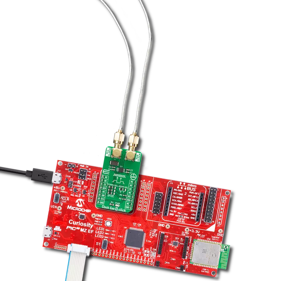
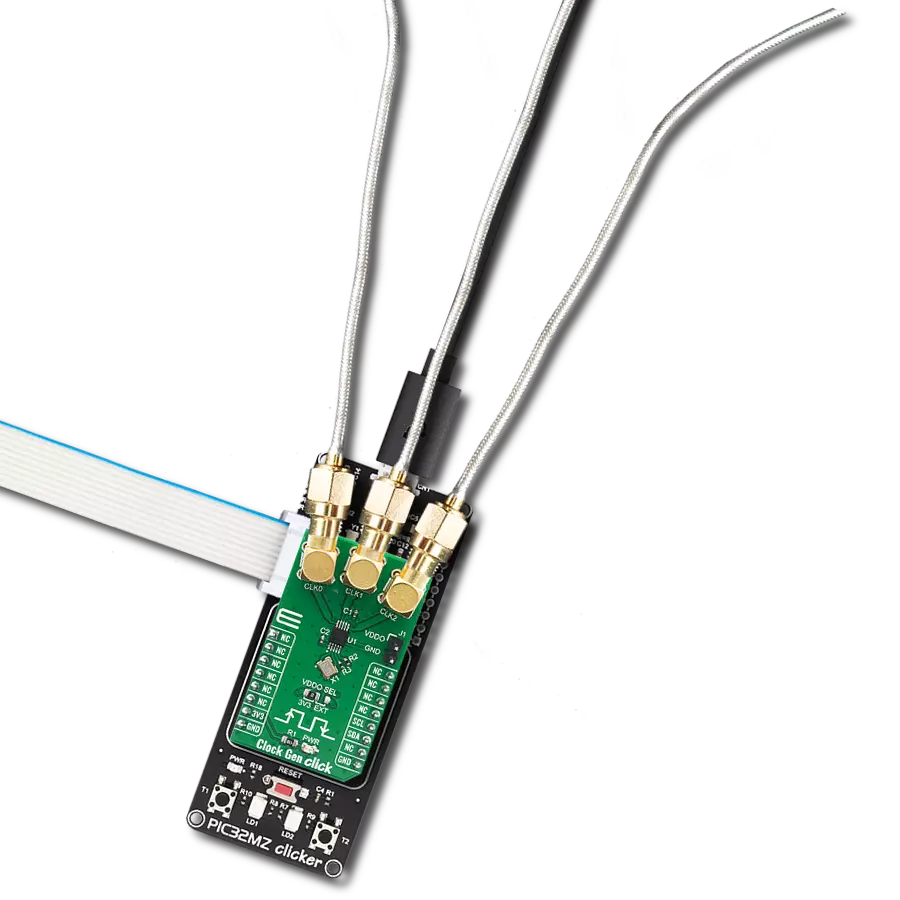
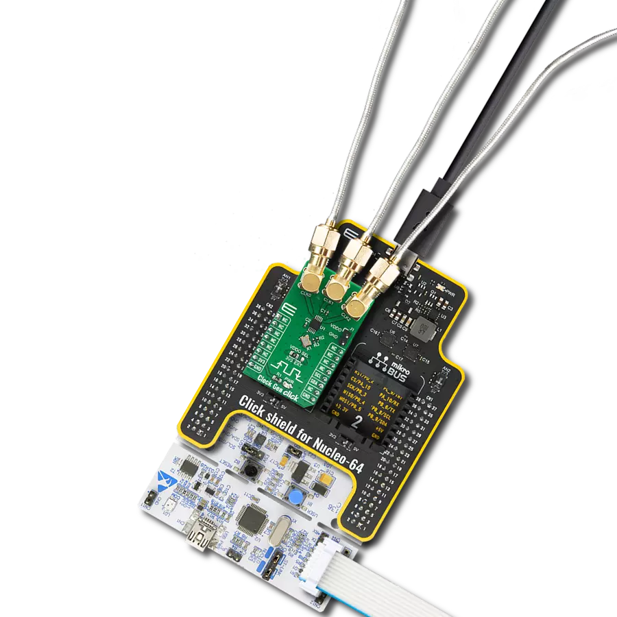
Clock Gen Click
Dev. board
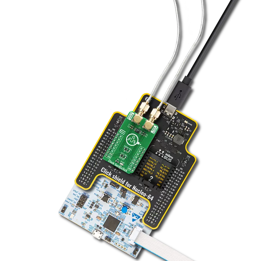
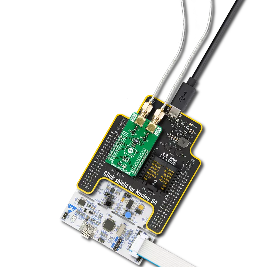
Nucleo-64 with STM32F091RC MCU
Compiler
NECTO Studio
MCU
STM32F091RC
Experience unmatched timing precision by integrating a reliable clock generator into your solution
A
A
Hardware Overview
How does it work?
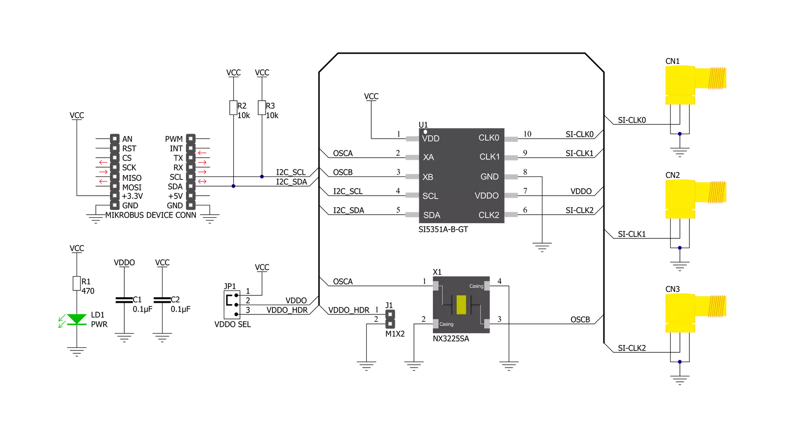
Clock Gen Click is based on the Si5351A, a versatile I2C programmable clock generator ideally suited for replacing crystals, crystal oscillators, VCXOs, PLLs, and buffers. The Si5351A consists of an input, two syntheses, and an output stage. The input stage accepts an external crystal (XTAL on XA and XB pins). The first stage of synthesis multiplies the input frequencies to a high-frequency intermediate clock, while the second stage of synthesis uses high-resolution MultiSynth fractional dividers to generate the desired output frequencies. Additional integer division is provided at the output stage for generating output frequencies as low as 2.5 kHz. Crosspoint switches at each synthesis stage allow total flexibility in routing any of the inputs to any of the outputs. Because of this high resolution and flexible synthesis architecture, the Si5351A can generate synchronous or free-running non-integer related clock frequencies at each output, enabling one device to synthesize clocks for multiple clock domains in a design. The Si5351A uses a fixed-frequency standard AT-cut crystal to reference the internal oscillator. The oscillator's output can
provide a free-running reference to one or both PLLs for generating asynchronous clocks. The oscillator's output frequency operates at the crystal frequency of 25 MHz. Internal load capacitors are provided to eliminate the need for external components when connecting a crystal to the Si5351A. The total internal XTAL load capacitance (CL) can be selected as 0, 6, 8, or 10 pF. The Si5351A uses two stages of synthesis to generate its final output clocks. The first stage uses PLLs to multiply the lower-frequency input references to a high-frequency intermediate clock. The second stage uses high-resolution MultiSynth fractional dividers to generate the required output frequencies. Only two unique frequencies above 112.5 MHz can be simultaneously output. For example, 125 MHz (CLK0), 130 MHz (CLK1), and 150 MHz (CLK2) are not allowed. Both PLLs are locked to the same source (XTAL). The crosspoint switch at the input of the second stage allows any of the MultiSynth dividers to connect to PLLA or PLLB. This flexible synthesis architecture allows any of the outputs to generate synchronous or non-synchronous clocks, with spread spectrum or
without spread spectrum, and with the flexibility of generating non-integer-related clock frequencies at each output. Frequencies down to 2.5 kHz can be generated by applying the R divider at the output of the Multisynth. All output drivers generate CMOS level outputs with a single output voltage supply pin (VDDO), allowing a different voltage signal level (1.8, 2.5, or 3.3 V) at the output banks. The output voltage level selection can be chosen by moving an SMD jumper labeled VDDO SEL to an appropriate position (3V3 or EXT). If 3V3 is chosen, the VDDO is supplied by the board. Otherwise, an external supply must be connected to the voltage level supply pin. This Click board™ uses the I2C communication interface and can be operated only with a 3.3V logic voltage level. The board must perform appropriate logic voltage level conversion before using MCUs with different logic levels. Also, it comes equipped with a library containing functions and an example code that can be used, as a reference, for further development.


Features overview
Development board
Nucleo-64 with STM32F091RC MCU offers a cost-effective and adaptable platform for developers to explore new ideas and prototype their designs. This board harnesses the versatility of the STM32 microcontroller, enabling users to select the optimal balance of performance and power consumption for their projects. It accommodates the STM32 microcontroller in the LQFP64 package and includes essential components such as a user LED, which doubles as an ARDUINO® signal, alongside user and reset push-buttons, and a 32.768kHz crystal oscillator for precise timing operations. Designed with expansion and flexibility in mind, the Nucleo-64 board features an ARDUINO® Uno V3 expansion connector and ST morpho extension pin
headers, granting complete access to the STM32's I/Os for comprehensive project integration. Power supply options are adaptable, supporting ST-LINK USB VBUS or external power sources, ensuring adaptability in various development environments. The board also has an on-board ST-LINK debugger/programmer with USB re-enumeration capability, simplifying the programming and debugging process. Moreover, the board is designed to simplify advanced development with its external SMPS for efficient Vcore logic supply, support for USB Device full speed or USB SNK/UFP full speed, and built-in cryptographic features, enhancing both the power efficiency and security of projects. Additional connectivity is
provided through dedicated connectors for external SMPS experimentation, a USB connector for the ST-LINK, and a MIPI® debug connector, expanding the possibilities for hardware interfacing and experimentation. Developers will find extensive support through comprehensive free software libraries and examples, courtesy of the STM32Cube MCU Package. This, combined with compatibility with a wide array of Integrated Development Environments (IDEs), including IAR Embedded Workbench®, MDK-ARM, and STM32CubeIDE, ensures a smooth and efficient development experience, allowing users to fully leverage the capabilities of the Nucleo-64 board in their projects.

Microcontroller Overview
MCU Card / MCU

Architecture
ARM Cortex-M0
MCU Memory (KB)
256
Silicon Vendor
STMicroelectronics
Pin count
64
RAM (Bytes)
32768
You complete me!
Accessories
Click Shield for Nucleo-64 comes equipped with two proprietary mikroBUS™ sockets, allowing all the Click board™ devices to be interfaced with the STM32 Nucleo-64 board with no effort. This way, Mikroe allows its users to add any functionality from our ever-growing range of Click boards™, such as WiFi, GSM, GPS, Bluetooth, ZigBee, environmental sensors, LEDs, speech recognition, motor control, movement sensors, and many more. More than 1537 Click boards™, which can be stacked and integrated, are at your disposal. The STM32 Nucleo-64 boards are based on the microcontrollers in 64-pin packages, a 32-bit MCU with an ARM Cortex M4 processor operating at 84MHz, 512Kb Flash, and 96KB SRAM, divided into two regions where the top section represents the ST-Link/V2 debugger and programmer while the bottom section of the board is an actual development board. These boards are controlled and powered conveniently through a USB connection to program and efficiently debug the Nucleo-64 board out of the box, with an additional USB cable connected to the USB mini port on the board. Most of the STM32 microcontroller pins are brought to the IO pins on the left and right edge of the board, which are then connected to two existing mikroBUS™ sockets. This Click Shield also has several switches that perform functions such as selecting the logic levels of analog signals on mikroBUS™ sockets and selecting logic voltage levels of the mikroBUS™ sockets themselves. Besides, the user is offered the possibility of using any Click board™ with the help of existing bidirectional level-shifting voltage translators, regardless of whether the Click board™ operates at a 3.3V or 5V logic voltage level. Once you connect the STM32 Nucleo-64 board with our Click Shield for Nucleo-64, you can access hundreds of Click boards™, working with 3.3V or 5V logic voltage levels.

Used MCU Pins
mikroBUS™ mapper
Take a closer look
Click board™ Schematic
Step by step
Project assembly
Start by selecting your development board and Click board™. Begin with the Nucleo-64 with STM32F091RC MCU as your development board.


Track your results in real time
Application Output
1. Application Output - In Debug mode, the 'Application Output' window enables real-time data monitoring, offering direct insight into execution results. Ensure proper data display by configuring the environment correctly using the provided tutorial.

2. UART Terminal - Use the UART Terminal to monitor data transmission via a USB to UART converter, allowing direct communication between the Click board™ and your development system. Configure the baud rate and other serial settings according to your project's requirements to ensure proper functionality. For step-by-step setup instructions, refer to the provided tutorial.

3. Plot Output - The Plot feature offers a powerful way to visualize real-time sensor data, enabling trend analysis, debugging, and comparison of multiple data points. To set it up correctly, follow the provided tutorial, which includes a step-by-step example of using the Plot feature to display Click board™ readings. To use the Plot feature in your code, use the function: plot(*insert_graph_name*, variable_name);. This is a general format, and it is up to the user to replace 'insert_graph_name' with the actual graph name and 'variable_name' with the parameter to be displayed.

Software Support
Library Description
This library contains API for Clock Gen Click driver.
Key functions:
clockgen_set_frequency- This function sets clock dividerclockgen_setup_pll- This function sets pllclockgen_setup_multisyinth- This function sets clock frequency on specific clock
Open Source
Code example
The complete application code and a ready-to-use project are available through the NECTO Studio Package Manager for direct installation in the NECTO Studio. The application code can also be found on the MIKROE GitHub account.
/*!
 * \file
 * \brief ClockGen Click example
 *
 * # Description
 * Clock Gen Click represent a replacement for crystals, crystal oscillators, VCXOs, phase-locked
 * loops (PLLs), and fanout buffers. This Click features an I2C configurable clock generator
 * based on a PLL + high resolution MultiSynth fractional divider architecture which can generate
 * any frequency up to 200 MHz with 0 ppm error. The chip on Click is capable of generating
 * synchronous or free-running non-integer related clock frequencies at each of its outputs
 * (CLK0, CLK1, and CLK2), enabling one device to synthesize clocks for multiple clock domains in a design.
 *
 * The demo application is composed of two sections :
 *
 * ## Application Init
 * Configures device to default function that enables clock 0 and disables all others.
 *
 * ## Application Task
 * Changes 4 different frequency in span of 5 seconds.
 *
 *
 * \author MikroE Team
 *
 */
// ------------------------------------------------------------------- INCLUDES

#include "board.h"
#include "log.h"
#include "clockgen.h"

// ------------------------------------------------------------------ VARIABLES

static clockgen_t clockgen;
static log_t logger;

// ------------------------------------------------------ APPLICATION FUNCTIONS

void application_init ( void )
{
    log_cfg_t log_cfg;
    clockgen_cfg_t cfg;

    /**
     * Logger initialization.
     * Default baud rate: 115200
     * Default log level: LOG_LEVEL_DEBUG
     * @note If USB_UART_RX and USB_UART_TX
     * are defined as HAL_PIN_NC, you will
     * need to define them manually for log to work.
     * See @b LOG_MAP_USB_UART macro definition for detailed explanation.
     */
    LOG_MAP_USB_UART( log_cfg );
    log_init( &logger, &log_cfg );
    log_info( &logger, "---- Application Init ----" );

    //  Click initialization.

    clockgen_cfg_setup( &cfg );
    CLOCKGEN_MAP_MIKROBUS( cfg, MIKROBUS_1 );
    clockgen_init( &clockgen, &cfg );

    clockgen_default_cfg( &clockgen );

    Delay_ms ( 500 );
}

void application_task ( void )
{
    clockgen_set_frequency( &clockgen, CLOCKGEN_CLOCK_0, CLOCKGEN_PLLA, 1 );
    Delay_ms ( 1000 );
    Delay_ms ( 1000 );
    Delay_ms ( 1000 );
    Delay_ms ( 1000 );
    Delay_ms ( 1000 );
    clockgen_set_frequency( &clockgen, CLOCKGEN_CLOCK_0, CLOCKGEN_PLLA, 3 );
    Delay_ms ( 1000 );
    Delay_ms ( 1000 );
    Delay_ms ( 1000 );
    Delay_ms ( 1000 );
    Delay_ms ( 1000 );
    clockgen_set_frequency( &clockgen, CLOCKGEN_CLOCK_0, CLOCKGEN_PLLA, 10 );
    Delay_ms ( 1000 );
    Delay_ms ( 1000 );
    Delay_ms ( 1000 );
    Delay_ms ( 1000 );
    Delay_ms ( 1000 );
    clockgen_set_frequency( &clockgen, CLOCKGEN_CLOCK_0, CLOCKGEN_PLLA, 5 );
    Delay_ms ( 1000 );
    Delay_ms ( 1000 );
    Delay_ms ( 1000 );
    Delay_ms ( 1000 );
    Delay_ms ( 1000 );
}

int main ( void )
{
    /* Do not remove this line or clock might not be set correctly. */
    #ifdef PREINIT_SUPPORTED
    preinit();
    #endif

    application_init( );

    for ( ; ; )
    {
        application_task( );
    }

    return 0;
}


// ------------------------------------------------------------------------ END
Additional Support
Resources
Category:Clock generator