Bring unprecedented accuracy and versatility to voltage control with MCP4361 and STM32F091RC
Ohm-inous possibilities

Published Feb 26, 2024
Click board™
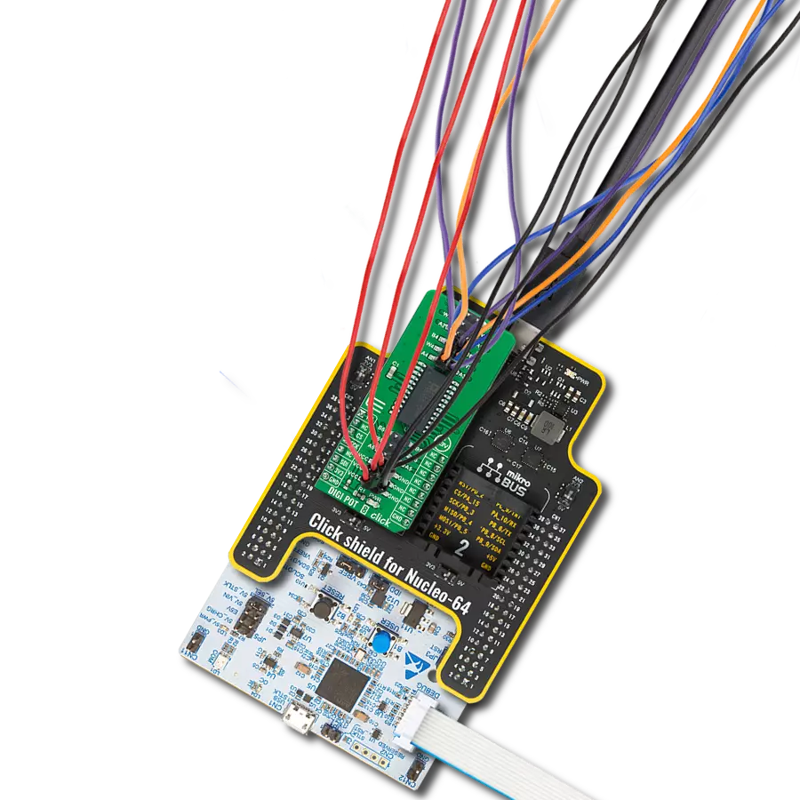
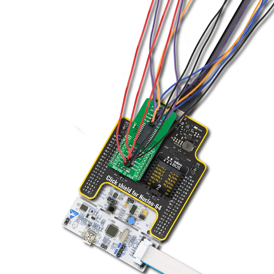
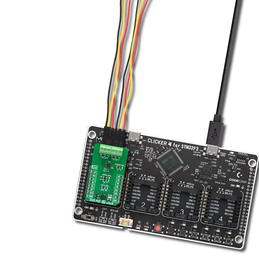
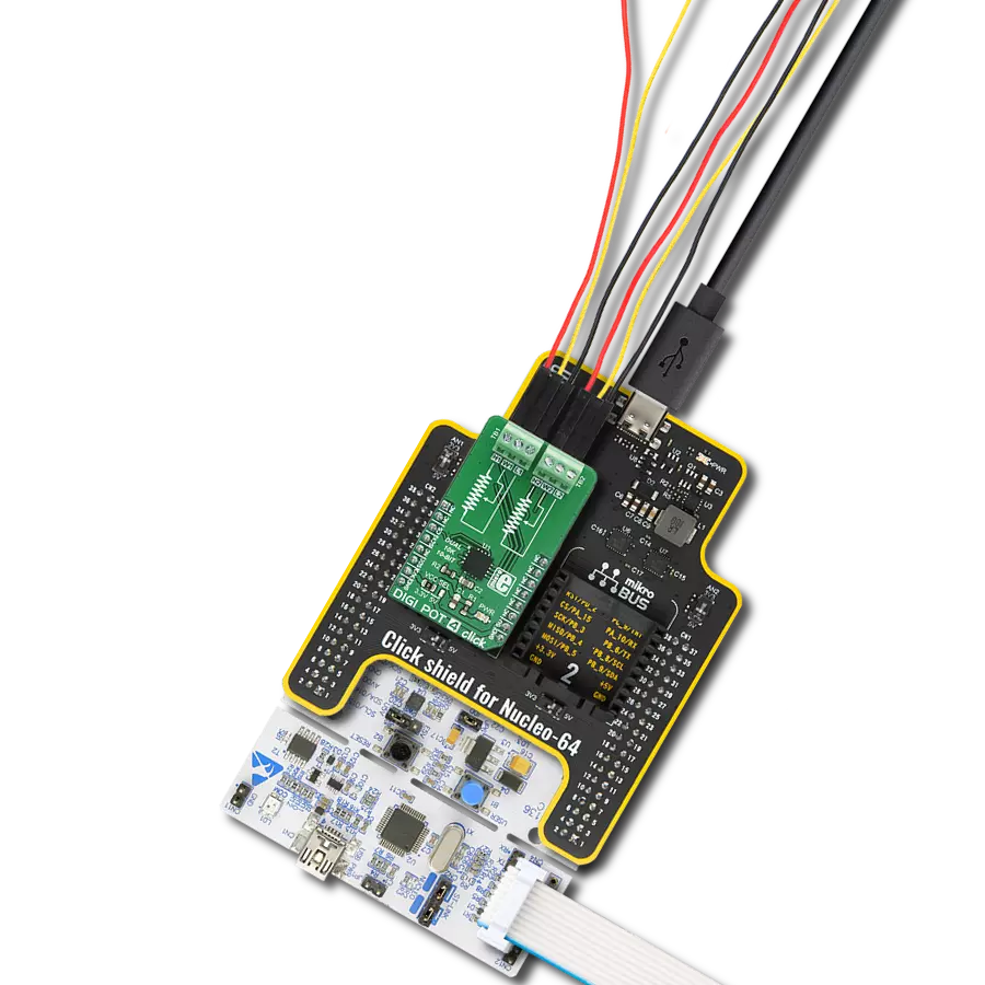
DIGI POT 5 click
Dev. board
Nucleo-64 with STM32F091RC MCU
Compiler
NECTO Studio
MCU
STM32F091RC
Replace cumbersome mechanical potentiometers with our digital alternative, improving reliability, durability, and allowing for advanced automation
A
A
Hardware Overview
How does it work?
DIGI POT 5 Click is based on the MCP4361, an 8-bit quad digital potentiometer from Microchip. This is a very versatile quad-digital potentiometer controlled via the SPI interface. The device has four integrated digital potentiometer sections, which consist of a string of resistors - serially connected, with digitally controlled analog switches, used to connect the wiper terminal position. The wiper position value of 0x000h corresponds to the lower end of the resistor ladder, while 0x100h corresponds to the upper end. These values can be written in the volatile wiper registers, with one address for each of the four wipers. Each of the four wipers can be controlled in several ways. Writing data directly to the volatile wiper register will move the wiper to the specified location. Wiper value can also be incremented or decremented by writing data to the incrementing or decrementing registers, providing that the wiper is not locked and that the wiper register value is not 0x000h (prevents further decrease) or above 0x100h (prevents further increase). Increasing and decreasing commands will be disregarded if the wiper register is set to a value greater than 0x100h. The incrementing and decrementing registers allow for less overhead if the wiper position has to be increased or decreased, making it easy to interface with the
rotary encoder applications, for example. The MCP4361 also features the WiperLock™ function, which prevents further changes in the wiper position, effectively locking the wiper in place. The CS pin must be pulled beyond the predefined voltage level threshold (8.5V to 12.5V) to enable this functionality. When this happens, the device enters the high voltage communication mode (HV mode), and the WiperLock™ functions can be accessed. The click board has a dedicated high-voltage input pad (VIHH), which can drive the CS pin with the appropriate voltage level when the HV mode is required. The resistor ladder network can be completely turned off by writing to the terminal control registers. This effectively disconnects the potentiometer terminals from a circuit, reducing the power consumption of the MCP4361 and the electrical circuit the IC is used in. The terminal control registers can switch the wiper terminals and the two resistor terminals separately. A STATUS register is also used for storing various status-related information, such as the WiperLock™ status, EEPROM writes to protect the status, and so on. The EEPROM memory holds the wiper data, even after the power is down. Several (five) general purpose 9bit addresses and 4 NV wiper register addresses are copied to the wiper register addresses after the restart or
power-up, allowing the device to resume the wiper position from a previous, stored state. By default, the data registers are zeroed out, while the NV wiper registers hold the middle scale position for the wiper. DIGI POT 5 Click has one 2x10 pin standard, 2.54mm pitch header connecting the four potentiometer terminals. There are three SMD jumpers onboard: The SMD jumper labeled WP is used to set the WP pin state of the MCP4361. The WP pin is used as the hardware EEPROM write protection and a software WP bit of the STATUS register (writable in HV mode only). The hardware WP pin and the software WP bit must be set to disabled mode to write to EEPROM. The SMD jumper labeled PWR SEL selects the power supply voltage - 3.3V or 5V. This also affects the logic voltage levels used for the SPI communication. The SMD jumper labeled CS SEL selects the CS pin voltage level. If the HV mode is required, this jumper should be moved to the VIHH position so that the externally connected 8.5V to 12.5V power source can pull up the CS pin. If HV mode is not required, this SMD jumper should stay at the default position (CS). Note that while in the HV mode, the CS pin is used the same way as with the regular SPI communication, with a difference in logical levels - the HV mode logical HIGH is at least 8.5V.

Features overview
Development board
Nucleo-64 with STM32F091RC MCU offers a cost-effective and adaptable platform for developers to explore new ideas and prototype their designs. This board harnesses the versatility of the STM32 microcontroller, enabling users to select the optimal balance of performance and power consumption for their projects. It accommodates the STM32 microcontroller in the LQFP64 package and includes essential components such as a user LED, which doubles as an ARDUINO® signal, alongside user and reset push-buttons, and a 32.768kHz crystal oscillator for precise timing operations. Designed with expansion and flexibility in mind, the Nucleo-64 board features an ARDUINO® Uno V3 expansion connector and ST morpho extension pin
headers, granting complete access to the STM32's I/Os for comprehensive project integration. Power supply options are adaptable, supporting ST-LINK USB VBUS or external power sources, ensuring adaptability in various development environments. The board also has an on-board ST-LINK debugger/programmer with USB re-enumeration capability, simplifying the programming and debugging process. Moreover, the board is designed to simplify advanced development with its external SMPS for efficient Vcore logic supply, support for USB Device full speed or USB SNK/UFP full speed, and built-in cryptographic features, enhancing both the power efficiency and security of projects. Additional connectivity is
provided through dedicated connectors for external SMPS experimentation, a USB connector for the ST-LINK, and a MIPI® debug connector, expanding the possibilities for hardware interfacing and experimentation. Developers will find extensive support through comprehensive free software libraries and examples, courtesy of the STM32Cube MCU Package. This, combined with compatibility with a wide array of Integrated Development Environments (IDEs), including IAR Embedded Workbench®, MDK-ARM, and STM32CubeIDE, ensures a smooth and efficient development experience, allowing users to fully leverage the capabilities of the Nucleo-64 board in their projects.

Microcontroller Overview
MCU Card / MCU

Architecture
ARM Cortex-M0
MCU Memory (KB)
256
Silicon Vendor
STMicroelectronics
Pin count
64
RAM (Bytes)
32768
You complete me!
Accessories
Click Shield for Nucleo-64 comes equipped with two proprietary mikroBUS™ sockets, allowing all the Click board™ devices to be interfaced with the STM32 Nucleo-64 board with no effort. This way, Mikroe allows its users to add any functionality from our ever-growing range of Click boards™, such as WiFi, GSM, GPS, Bluetooth, ZigBee, environmental sensors, LEDs, speech recognition, motor control, movement sensors, and many more. More than 1537 Click boards™, which can be stacked and integrated, are at your disposal. The STM32 Nucleo-64 boards are based on the microcontrollers in 64-pin packages, a 32-bit MCU with an ARM Cortex M4 processor operating at 84MHz, 512Kb Flash, and 96KB SRAM, divided into two regions where the top section represents the ST-Link/V2 debugger and programmer while the bottom section of the board is an actual development board. These boards are controlled and powered conveniently through a USB connection to program and efficiently debug the Nucleo-64 board out of the box, with an additional USB cable connected to the USB mini port on the board. Most of the STM32 microcontroller pins are brought to the IO pins on the left and right edge of the board, which are then connected to two existing mikroBUS™ sockets. This Click Shield also has several switches that perform functions such as selecting the logic levels of analog signals on mikroBUS™ sockets and selecting logic voltage levels of the mikroBUS™ sockets themselves. Besides, the user is offered the possibility of using any Click board™ with the help of existing bidirectional level-shifting voltage translators, regardless of whether the Click board™ operates at a 3.3V or 5V logic voltage level. Once you connect the STM32 Nucleo-64 board with our Click Shield for Nucleo-64, you can access hundreds of Click boards™, working with 3.3V or 5V logic voltage levels.

Used MCU Pins
mikroBUS™ mapper
Take a closer look
Click board™ Schematic

Step by step
Project assembly
Start by selecting your development board and Click board™. Begin with the Nucleo-64 with STM32F091RC MCU as your development board.


Software Support
Library Description
This library contains API for DIGI POT 5 Click driver.
Key functions:
digipot5_generic_write- Generic Write functiondigipot5_generic_read- Generic Read functiondigipot5_increment_wiper- Increment Wiper function
Open Source
Code example
The complete application code and a ready-to-use project are available through the NECTO Studio Package Manager for direct installation in the NECTO Studio. The application code can also be found on the MIKROE GitHub account.
/*!
 * \file main.c
 * \brief DIGI POT 5 Click example
 *
 * # Description
 * This example demonstrates the use of the DIGI POT 5 Click board.
 *
 * The demo application is composed of two sections :
 *
 * ## Application Init
 * Initializes all necessary peripherals and pins used for the DIGI POT 5 Click.
 * Also allows the device to be reset and configured to enable all wipers (4).
 * UART console module will be initialized also in this function.
 *
 * ## Application Task
 * Demonstrates the use of Click driver functions by performing a control of
 * the all wipers positions. By checking the uart console, user can be informed
 * about the all current wipers positions.
 *
 * *note:*
 * Increment/decrement command can be issued only to volatile wiper locations.
 *
 * \author Nemanja Medakovic
 *
 */
// ------------------------------------------------------------------- INCLUDES

#include "board.h"
#include "log.h"
#include "digipot5.h"


// ------------------------------------------------------------------ VARIABLES

static digipot5_t digipot5;
static log_t console;
static uint8_t i;

// ------------------------------------------------------ APPLICATION FUNCTIONS

void application_init( void )
{
    digipot5_cfg_t digipot5_cfg;
    log_cfg_t console_cfg;

    //  Click initialization.
    digipot5_cfg_setup( &digipot5_cfg );
    DIGIPOT5_MAP_MIKROBUS( digipot5_cfg, MIKROBUS_1 );
    digipot5_init( &digipot5, &digipot5_cfg );
    digipot5_reset( &digipot5 );
    digipot5_default_cfg( &digipot5 );

    /**
     * Logger initialization.
     * Default baud rate: 115200
     * Default log level: LOG_LEVEL_DEBUG
     * @note If USB_UART_RX and USB_UART_TX
     * are defined as HAL_PIN_NC, you will
     * need to define them manually for log to work.
     * See @b LOG_MAP_USB_UART macro definition for detailed explanation.
     */
    LOG_MAP_USB_UART( console_cfg );
    log_init( &console, &console_cfg );
    log_printf( &console, "***  DIGI POT 5 Initialization Done  ***\r\n" );
    log_printf( &console, "****************************************\r\n" );
}

void application_task( void )
{
    log_printf( &console, "* Setting wiper 0 to zero scale.\r\n" );
    digipot5_generic_write( &digipot5, DIGIPOT5_REG_WIPER0_VOL,
                            DIGIPOT5_RES_ZEROSCALE );
    log_printf( &console, "* Setting wiper 1 to 3k Ohm.\r\n" );
    digipot5_generic_write( &digipot5, DIGIPOT5_REG_WIPER1_VOL,
                            DIGIPOT5_RES_3KOHM );
    log_printf( &console, "* Setting wiper 2 to half scale (5k Ohm).\r\n" );
    digipot5_generic_write( &digipot5, DIGIPOT5_REG_WIPER2_VOL,
                            DIGIPOT5_RES_5KOHM_HALFSCALE );
    log_printf( &console, "* Setting wiper 3 to full scale (10k Ohm).\r\n" );
    digipot5_generic_write( &digipot5, DIGIPOT5_REG_WIPER3_VOL,
                            DIGIPOT5_RES_10KOHM_FULLSCALE );

    Delay_ms ( 1000 );
    Delay_ms ( 1000 );
    Delay_ms ( 1000 );
    log_printf( &console, "* Decrementing wiper 3 by 5 steps.\r\n" );
    for ( i = 0; i < 5; i++ )
    {
        digipot5_decrement_wiper( &digipot5, DIGIPOT5_REG_WIPER3_VOL );
    }

    Delay_ms ( 1000 );
    Delay_ms ( 1000 );
    Delay_ms ( 1000 );
    log_printf( &console, "* Incrementing wiper 0 by 10 steps.\r\n" );
    for ( i = 0; i < 10; i++ )
    {
        digipot5_increment_wiper( &digipot5, DIGIPOT5_REG_WIPER0_VOL );
    }

    Delay_ms ( 1000 );
    Delay_ms ( 1000 );
    Delay_ms ( 1000 );
    log_printf( &console, "* Setting wiper 0 to 2k Ohm.\r\n" );
    digipot5_generic_write( &digipot5, DIGIPOT5_REG_WIPER0_VOL,
                            DIGIPOT5_RES_2KOHM );
    log_printf( &console, "* Setting wiper 1 to 2k Ohm.\r\n" );
    digipot5_generic_write( &digipot5, DIGIPOT5_REG_WIPER1_VOL,
                            DIGIPOT5_RES_2KOHM );
    log_printf( &console, "* Setting wiper 2 to 2k Ohm.\r\n" );
    digipot5_generic_write( &digipot5, DIGIPOT5_REG_WIPER2_VOL,
                            DIGIPOT5_RES_2KOHM );
    log_printf( &console, "* Setting wiper 3 to 2k Ohm.\r\n" );
    digipot5_generic_write( &digipot5, DIGIPOT5_REG_WIPER3_VOL,
                            DIGIPOT5_RES_2KOHM );

    Delay_ms ( 1000 );
    Delay_ms ( 1000 );
    Delay_ms ( 1000 );
    log_printf( &console, "****************************************\r\n" );
}

int main ( void )
{
    /* Do not remove this line or clock might not be set correctly. */
    #ifdef PREINIT_SUPPORTED
    preinit();
    #endif

    application_init( );

    for ( ; ; )
    {
        application_task( );
    }

    return 0;
}


// ------------------------------------------------------------------------ END
Additional Support
Resources
Category:Digital potentiometer