Navigate any terrain with precision and ease using ORG1511 and STM32F091RC
Your world with pinpoint accuracy!

Published Feb 26, 2024
Click board™
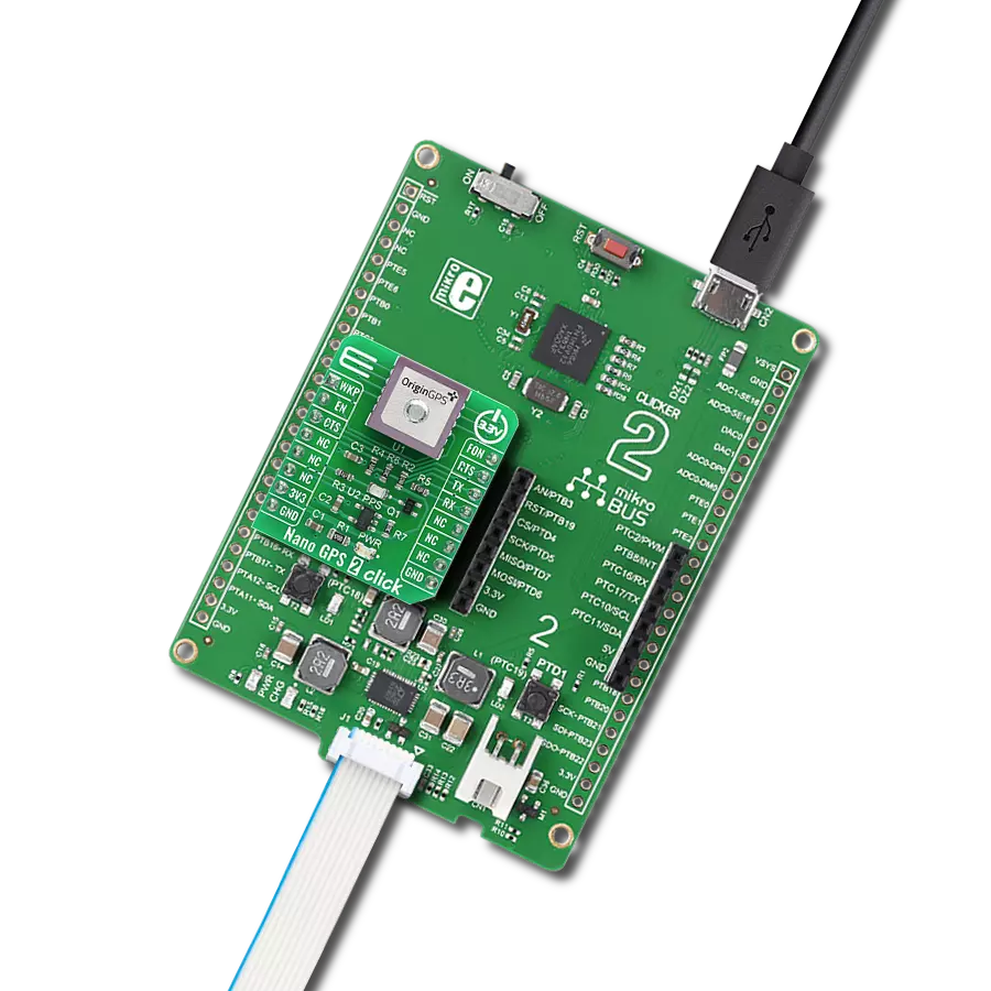
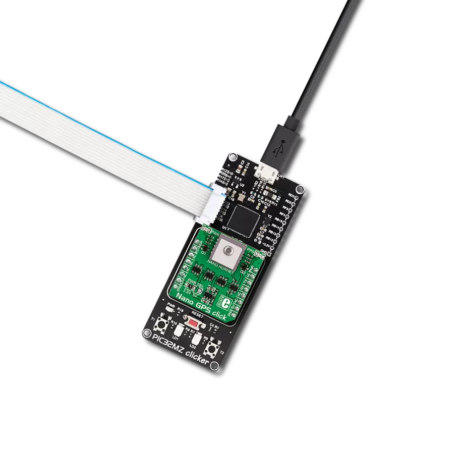
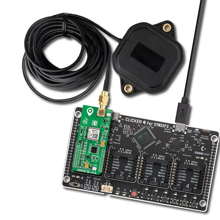
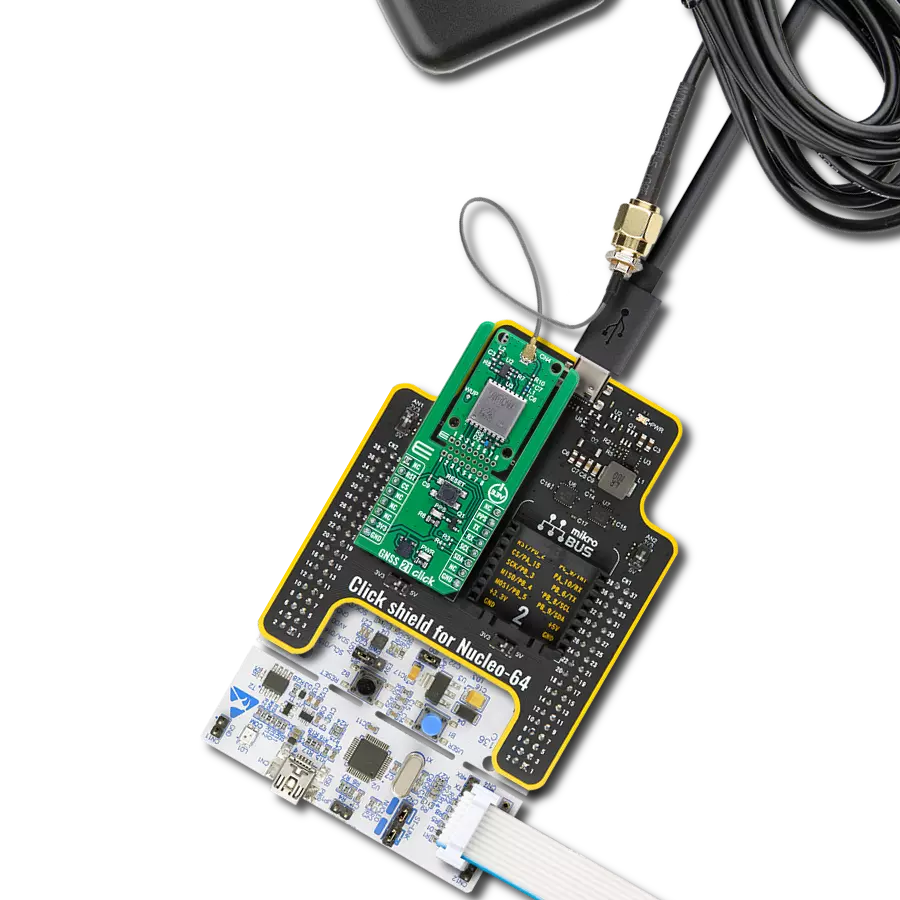
Nano GPS 3 Click
Dev. board
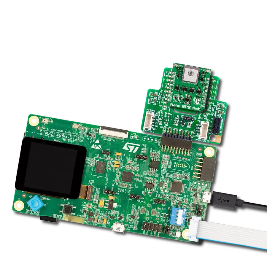
Nucleo-64 with STM32F091RC MCU
Compiler
NECTO Studio
MCU
STM32F091RC
Experience the future of navigation with our GPS/GNSS solution, designed to provide seamless, reliable location data for applications that demand precision and efficiency.
A
A
Hardware Overview
How does it work?
Nano GPS 3 Click is based on the ORG1511, a GPS/GNSS module with an integrated antenna from OriginGPS. It is built around MediaTek’s MT3333 SoC, which includes an 8Mb built-in flash, GNSS radio, a DSP core for processing the GNSS signal, a navigation subsystem, a peripheral controller, and a PMU subsystem. The module is 10x10 mm, the industry’s smallest global positioning module, with superior sensitivity and outstanding performance. It can achieve time to first fix (TTFF) in less than one second, location accuracy of approximately two meters, and tracking sensitivity of -165dBm. Its architecture can detect changes in context, temperature, and satellite signals to achieve a state of near-continuous availability by maintaining and updating its internal parameters, such as time, frequency, and satellite ephemeris data. An on-board patch antenna is built from a Hi-K ceramic element and is accompanied by a GNSS SAW Filter and a GNSS dual-stage LNA, which amplifies the GNSS signal to meet the RF down converter
input threshold. The ORG1511 operates in the 1560 up to 1620MHz frequency range and has 99 search channels and 33 simultaneous tracking channels. Additionally, the module features jamming rejection, indoor and outdoor multipath, cross-correlation mitigation, static navigation, assisted navigation, SBAS, DGPS, and more. It can work in full-power continuous, standby, periodic, and AlwaysLocateTM modes. The Nano GPS 3 Click is equipped with a backup battery JST connector as an optional backup power supply. Please note that JST battery connectors are not standardized, so check the polarity before connecting. Another feature of this Click board™ is the Backup Mode that can be entered by the software NMEA command, forcing the module to enter the Idle state. You can also enter the Backup Mode over the BCKM SEL switch, thus disconnecting the VCC power supply. The battery should be connected before switching it to the Backup Mode over the switch. Worth mentioning is a 1PPS LED as a pulse-per-second signal that provides a pulse
signal for timing purposes. Nano GPS 3 Click can use a standard 2-Wire I2C interface to communicate with the host MCU, supporting clock speeds of 400kHz. In addition, over the COMM SEL jumper, you can select a standard UART interface to communicate with the host MCU with commonly used UART RX and TX pins and additional UART RTS and CTS control flow pins. The communication supports a default baud rate of 9600bps. The WUP pin is an output-only for probing to determine if the module is in active mode or Standby/Backup states. With the FON pin (force-on), you can control the power states of the module, say, returning from a backup mode to a full power mode. This Click board™ can be operated only with a 3.3V logic voltage level. The board must perform appropriate logic voltage level conversion before using MCUs with different logic levels. Also, this Click board™ comes equipped with a library containing easy-to-use functions and an example code that can be used as a reference for further development.

Features overview
Development board
Nucleo-64 with STM32F091RC MCU offers a cost-effective and adaptable platform for developers to explore new ideas and prototype their designs. This board harnesses the versatility of the STM32 microcontroller, enabling users to select the optimal balance of performance and power consumption for their projects. It accommodates the STM32 microcontroller in the LQFP64 package and includes essential components such as a user LED, which doubles as an ARDUINO® signal, alongside user and reset push-buttons, and a 32.768kHz crystal oscillator for precise timing operations. Designed with expansion and flexibility in mind, the Nucleo-64 board features an ARDUINO® Uno V3 expansion connector and ST morpho extension pin
headers, granting complete access to the STM32's I/Os for comprehensive project integration. Power supply options are adaptable, supporting ST-LINK USB VBUS or external power sources, ensuring adaptability in various development environments. The board also has an on-board ST-LINK debugger/programmer with USB re-enumeration capability, simplifying the programming and debugging process. Moreover, the board is designed to simplify advanced development with its external SMPS for efficient Vcore logic supply, support for USB Device full speed or USB SNK/UFP full speed, and built-in cryptographic features, enhancing both the power efficiency and security of projects. Additional connectivity is
provided through dedicated connectors for external SMPS experimentation, a USB connector for the ST-LINK, and a MIPI® debug connector, expanding the possibilities for hardware interfacing and experimentation. Developers will find extensive support through comprehensive free software libraries and examples, courtesy of the STM32Cube MCU Package. This, combined with compatibility with a wide array of Integrated Development Environments (IDEs), including IAR Embedded Workbench®, MDK-ARM, and STM32CubeIDE, ensures a smooth and efficient development experience, allowing users to fully leverage the capabilities of the Nucleo-64 board in their projects.

Microcontroller Overview
MCU Card / MCU

Architecture
ARM Cortex-M0
MCU Memory (KB)
256
Silicon Vendor
STMicroelectronics
Pin count
64
RAM (Bytes)
32768
You complete me!
Accessories
Click Shield for Nucleo-64 comes equipped with two proprietary mikroBUS™ sockets, allowing all the Click board™ devices to be interfaced with the STM32 Nucleo-64 board with no effort. This way, Mikroe allows its users to add any functionality from our ever-growing range of Click boards™, such as WiFi, GSM, GPS, Bluetooth, ZigBee, environmental sensors, LEDs, speech recognition, motor control, movement sensors, and many more. More than 1537 Click boards™, which can be stacked and integrated, are at your disposal. The STM32 Nucleo-64 boards are based on the microcontrollers in 64-pin packages, a 32-bit MCU with an ARM Cortex M4 processor operating at 84MHz, 512Kb Flash, and 96KB SRAM, divided into two regions where the top section represents the ST-Link/V2 debugger and programmer while the bottom section of the board is an actual development board. These boards are controlled and powered conveniently through a USB connection to program and efficiently debug the Nucleo-64 board out of the box, with an additional USB cable connected to the USB mini port on the board. Most of the STM32 microcontroller pins are brought to the IO pins on the left and right edge of the board, which are then connected to two existing mikroBUS™ sockets. This Click Shield also has several switches that perform functions such as selecting the logic levels of analog signals on mikroBUS™ sockets and selecting logic voltage levels of the mikroBUS™ sockets themselves. Besides, the user is offered the possibility of using any Click board™ with the help of existing bidirectional level-shifting voltage translators, regardless of whether the Click board™ operates at a 3.3V or 5V logic voltage level. Once you connect the STM32 Nucleo-64 board with our Click Shield for Nucleo-64, you can access hundreds of Click boards™, working with 3.3V or 5V logic voltage levels.

Used MCU Pins
mikroBUS™ mapper
Take a closer look
Click board™ Schematic

Step by step
Project assembly
Start by selecting your development board and Click board™. Begin with the Nucleo-64 with STM32F091RC MCU as your development board.


Software Support
Library Description
This library contains API for Nano GPS 3 Click driver.
Key functions:
nanogps3_parse_gngga- Nano GPS 3 parse GNGGA function.nanogps3_generic_read- Nano GPS 3 data reading function.nanogps3_generic_write- Nano GPS 3 data writing function.
Open Source
Code example
The complete application code and a ready-to-use project are available through the NECTO Studio Package Manager for direct installation in the NECTO Studio. The application code can also be found on the MIKROE GitHub account.
/*!
 * @file main.c
 * @brief Nano GPS 3 Click example
 *
 * # Description
 * This example demonstrates the use of Nano GPS 3 Click by reading and displaying
 * the GPS coordinates.
 *
 * The demo application is composed of two sections :
 *
 * ## Application Init
 * Initializes the driver and resets the Click board.
 *
 * ## Application Task
 * Reads the received data, parses the GNGGA info from it, and once it receives the position fix
 * it will start displaying the coordinates on the USB UART.
 *
 * ## Additional Function
 * - static void nanogps3_clear_app_buf ( void )
 * - static err_t nanogps3_process ( nanogps3_t *ctx )
 * - static void nanogps3_parser_application ( char *rsp )
 *
 * @author Nenad Filipovic
 *
 */

#include "board.h"
#include "log.h"
#include "nanogps3.h"

static nanogps3_t nanogps3;
static log_t logger;

static char app_buf[ NANOGPS3_RX_DRV_BUFFER_SIZE ];
static int32_t app_buf_len = 0;

/**
 * @brief Nano GPS 3 clearing application buffer.
 * @details This function clears memory of application buffer and reset its length.
 * @return None.
 * @note None.
 */
static void nanogps3_clear_app_buf ( void );

/**
 * @brief Nano GPS 3 data reading function.
 * @details This function reads data from device and concatenates data to application buffer.
 * @param[in] ctx : Click context object.
 * See #nanogps3_t object definition for detailed explanation.
 * @return @li @c  0 - Read some data.
 *         @li @c -1 - Nothing is read or Application buffer overflow.
 * @note None.
 */
static err_t nanogps3_process ( nanogps3_t *ctx );

/**
 * @brief Nano GPS 3 parser application.
 * @param[in] rsp Response buffer.
 * @details This function logs GNSS data on the USB UART.
 * @return None.
 * @note None.
 */
static void nanogps3_parser_application ( char *rsp );

void application_init ( void )
{
    log_cfg_t log_cfg;  /**< Logger config object. */
    nanogps3_cfg_t nanogps3_cfg;  /**< Click config object. */

    /**
     * Logger initialization.
     * Default baud rate: 115200
     * Default log level: LOG_LEVEL_DEBUG
     * @note If USB_UART_RX and USB_UART_TX
     * are defined as HAL_PIN_NC, you will
     * need to define them manually for log to work.
     * See @b LOG_MAP_USB_UART macro definition for detailed explanation.
     */
    LOG_MAP_USB_UART( log_cfg );
    log_init( &logger, &log_cfg );
    log_info( &logger, " Application Init " );

    // Click initialization.
    nanogps3_cfg_setup( &nanogps3_cfg );
    NANOGPS3_MAP_MIKROBUS( nanogps3_cfg, MIKROBUS_1 );
    err_t init_flag = nanogps3_init( &nanogps3, &nanogps3_cfg );
    if ( ( UART_ERROR == init_flag ) || ( I2C_MASTER_ERROR == init_flag ) )
    {
        log_error( &logger, " Communication init." );
        for ( ; ; );
    }

    nanogps3_default_cfg( &nanogps3 );
    log_info( &logger, " Application Task " );
}

void application_task ( void )
{
    nanogps3_process( &nanogps3 );
    if ( app_buf_len > ( sizeof( NANOGPS3_RSP_GNGGA ) + NANOGPS3_NMEA_GNGGA_NUM_ELEMENT ) )
    {
        nanogps3_parser_application( app_buf );
    }
}

int main ( void )
{
    /* Do not remove this line or clock might not be set correctly. */
    #ifdef PREINIT_SUPPORTED
    preinit();
    #endif

    application_init( );

    for ( ; ; )
    {
        application_task( );
    }

    return 0;
}

static void nanogps3_clear_app_buf ( void )
{
    memset( app_buf, 0, app_buf_len );
    app_buf_len = 0;
}

static err_t nanogps3_process ( nanogps3_t *ctx )
{
    int32_t rx_size;
    char rx_buf[ NANOGPS3_RX_DRV_BUFFER_SIZE ] = { 0 };

    if ( NANOGPS3_DRV_SEL_UART == ctx->drv_sel )
    {
        rx_size = nanogps3_generic_read( &nanogps3, &rx_buf, NANOGPS3_RX_DRV_BUFFER_SIZE );
    }
    else
    {
        if ( NANOGPS3_OK == nanogps3_generic_read( ctx, rx_buf, 1 ) )
        {
            if ( NANOGPS3_DUMMY != rx_buf[ 0 ] )
            {
                rx_size = 1;
            }
        }
    }
    if ( rx_size > 0 )
    {
        int32_t buf_cnt = 0;
        if ( ( app_buf_len + rx_size ) > NANOGPS3_RX_DRV_BUFFER_SIZE )
        {
            nanogps3_clear_app_buf( );
            return NANOGPS3_ERROR;
        }
        else
        {
            buf_cnt = app_buf_len;
            app_buf_len += rx_size;
        }
        for ( int32_t rx_cnt = 0; rx_cnt < rx_size; rx_cnt++ )
        {
            if ( rx_buf[ rx_cnt ] )
            {
                app_buf[ ( buf_cnt + rx_cnt ) ] = rx_buf[ rx_cnt ];
            }
            else
            {
                app_buf_len--;
                buf_cnt--;
            }
        }
        return NANOGPS3_OK;
    }
    return NANOGPS3_ERROR;
}

static void nanogps3_parser_application ( char *rsp )
{
    char element_buf[ 100 ] = { 0 };
    if ( NANOGPS3_OK == nanogps3_parse_gngga( rsp, NANOGPS3_GNGGA_LATITUDE, element_buf ) )
    {
        static uint8_t wait_for_fix_cnt = 0;
        if ( 0 < strlen( element_buf ) > 0 )
        {
            log_printf( &logger, "\r\n Latitude: %.2s degrees, %s minutes \r\n",
                        element_buf, &element_buf[ 2 ] );
            nanogps3_parse_gngga( rsp, NANOGPS3_GNGGA_LONGITUDE, element_buf );
            log_printf( &logger, " Longitude: %.3s degrees, %s minutes \r\n",
                        element_buf, &element_buf[ 3 ] );
            memset( element_buf, 0, sizeof( element_buf ) );
            nanogps3_parse_gngga( rsp, NANOGPS3_GNGGA_ALTITUDE, element_buf );
            log_printf( &logger, " Altitude: %s m \r\n", element_buf );
            wait_for_fix_cnt = 0;
        }
        else
        {
            if ( wait_for_fix_cnt % 5 == 0 )
            {
                log_printf( &logger, " Waiting for the position fix...\r\n\n" );
                wait_for_fix_cnt = 0;
            }
            wait_for_fix_cnt++;
        }
        nanogps3_clear_app_buf(  );
    }
}

// ------------------------------------------------------------------------ END
Additional Support
Resources
Category:GPS/GNSS