Generate high-frequency clock output with ICS501 and STM32F091RC
Phase-Locked Loop (PLL) mechanism

Published Feb 26, 2024
Click board™
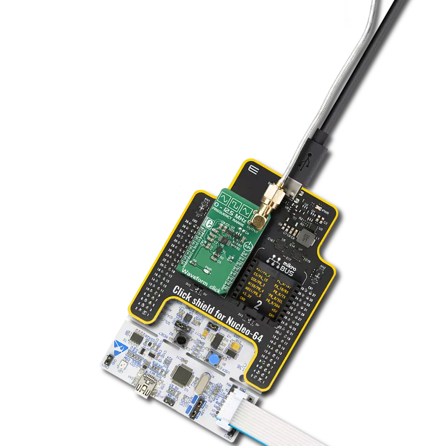
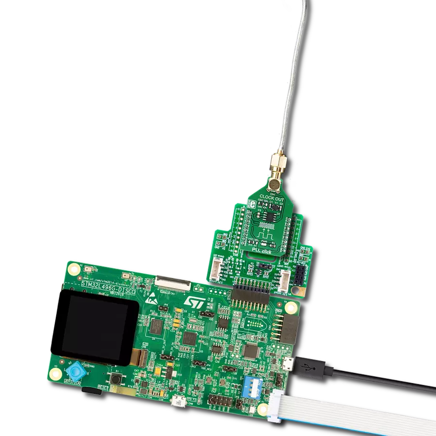
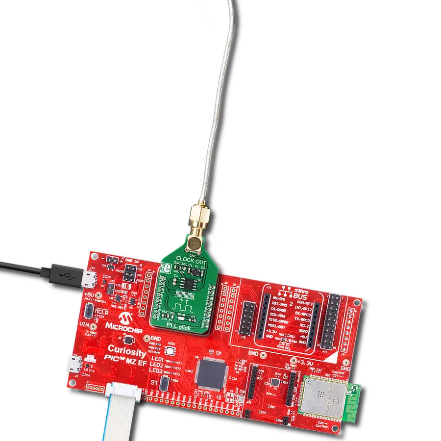
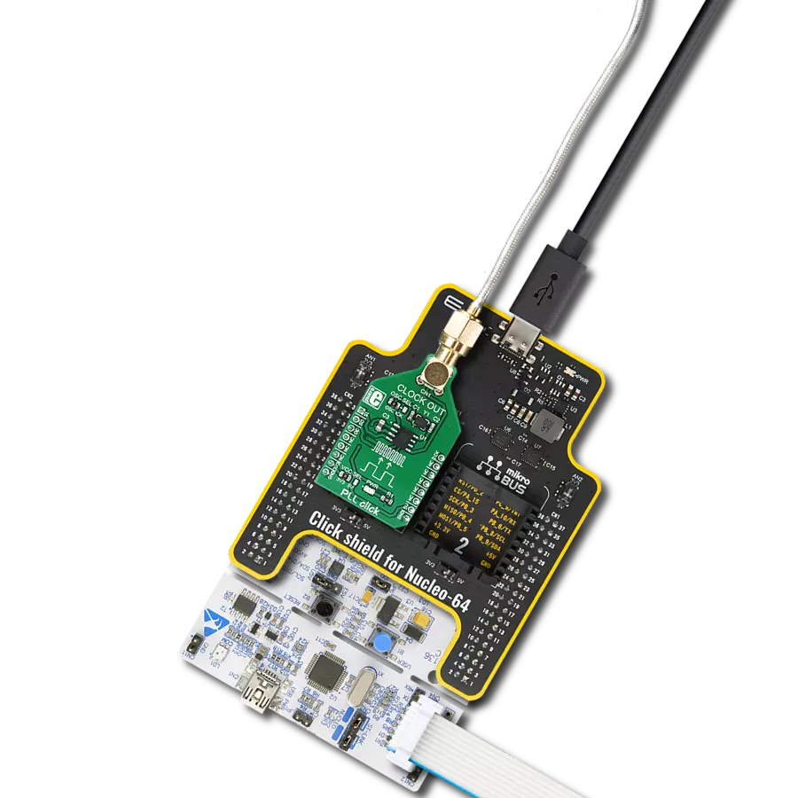
PLL Click
Dev. board
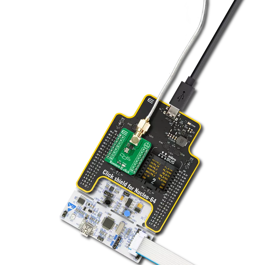
Nucleo-64 with STM32F091RC MCU
Compiler
NECTO Studio
MCU
STM32F091RC
Generate highly stable and coherent high-frequency signals for applications requiring tight synchronization and minimal phase noise
A
A
Hardware Overview
How does it work?
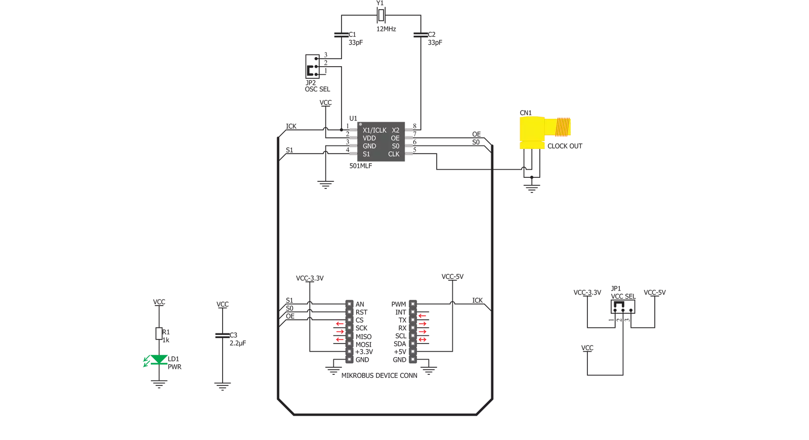
PLL Click is based on the ICS501, a LOCO™ PLL clock multiplier, from Integrated Device Technology. This IC uses the Phase-Locked Loop to provide a high-frequency clock output, deriving input from a much cheaper, standard fundamental frequency crystal oscillator. Besides the onboard crystal oscillator fixed at 12MHz, it is possible to select the signal from the mikroBUS™ PWM pin as the clock input source. To select the desired multiplication factor, the states of the two input pins, S0 and S1, are routed to the mikroBUS™ pins RST and AN, respectively. These pins can be set to a HIGH or LOW logic state or disconnected (by tri-stating the MCU pins). The combination of these pins states will set the PLL
Click to a specific multiplier. The Output Enable (OE) pin of the ICS501 is used to turn off the output clock by setting it to a LOW logic level. It will additionally set the clock output pin in high impedance (Hi-Z) mode, allowing complete disconnection and no influence on the rest of the circuit, which is useful for experimenting and prototyping purposes. This pin is internally pulled to a HIGH logic level. The OE pin is routed to the CS pin of the mikroBUS™. PLL Click is equipped with two onboard SMD jumpers. The SMD jumper labeled as the VCC SEL is used to select the operating voltage level, consequently limiting the amplitude of the clock output signal with respect to the selected voltage. The other SMD jumper
labeled as the OSC SEL chooses the clock input source between the onboard 12MHz crystal oscillator or the external clock signal. The output signal is routed through the onboard SMA connector, which provides a secure connection and good signal shielding. PLL Click has a library containing functions for all the MIKROE compilers (mikroBASIC, mikroPASCAL, and mikroC). Although relatively easy to control, the library offers comprehensive functions that make the code readable and easy to use. The included example application demonstrates the use of these functions, and it can be used as a reference for custom projects.

Features overview
Development board
Nucleo-64 with STM32F091RC MCU offers a cost-effective and adaptable platform for developers to explore new ideas and prototype their designs. This board harnesses the versatility of the STM32 microcontroller, enabling users to select the optimal balance of performance and power consumption for their projects. It accommodates the STM32 microcontroller in the LQFP64 package and includes essential components such as a user LED, which doubles as an ARDUINO® signal, alongside user and reset push-buttons, and a 32.768kHz crystal oscillator for precise timing operations. Designed with expansion and flexibility in mind, the Nucleo-64 board features an ARDUINO® Uno V3 expansion connector and ST morpho extension pin
headers, granting complete access to the STM32's I/Os for comprehensive project integration. Power supply options are adaptable, supporting ST-LINK USB VBUS or external power sources, ensuring adaptability in various development environments. The board also has an on-board ST-LINK debugger/programmer with USB re-enumeration capability, simplifying the programming and debugging process. Moreover, the board is designed to simplify advanced development with its external SMPS for efficient Vcore logic supply, support for USB Device full speed or USB SNK/UFP full speed, and built-in cryptographic features, enhancing both the power efficiency and security of projects. Additional connectivity is
provided through dedicated connectors for external SMPS experimentation, a USB connector for the ST-LINK, and a MIPI® debug connector, expanding the possibilities for hardware interfacing and experimentation. Developers will find extensive support through comprehensive free software libraries and examples, courtesy of the STM32Cube MCU Package. This, combined with compatibility with a wide array of Integrated Development Environments (IDEs), including IAR Embedded Workbench®, MDK-ARM, and STM32CubeIDE, ensures a smooth and efficient development experience, allowing users to fully leverage the capabilities of the Nucleo-64 board in their projects.

Microcontroller Overview
MCU Card / MCU

Architecture
ARM Cortex-M0
MCU Memory (KB)
256
Silicon Vendor
STMicroelectronics
Pin count
64
RAM (Bytes)
32768
You complete me!
Accessories
Click Shield for Nucleo-64 comes equipped with two proprietary mikroBUS™ sockets, allowing all the Click board™ devices to be interfaced with the STM32 Nucleo-64 board with no effort. This way, Mikroe allows its users to add any functionality from our ever-growing range of Click boards™, such as WiFi, GSM, GPS, Bluetooth, ZigBee, environmental sensors, LEDs, speech recognition, motor control, movement sensors, and many more. More than 1537 Click boards™, which can be stacked and integrated, are at your disposal. The STM32 Nucleo-64 boards are based on the microcontrollers in 64-pin packages, a 32-bit MCU with an ARM Cortex M4 processor operating at 84MHz, 512Kb Flash, and 96KB SRAM, divided into two regions where the top section represents the ST-Link/V2 debugger and programmer while the bottom section of the board is an actual development board. These boards are controlled and powered conveniently through a USB connection to program and efficiently debug the Nucleo-64 board out of the box, with an additional USB cable connected to the USB mini port on the board. Most of the STM32 microcontroller pins are brought to the IO pins on the left and right edge of the board, which are then connected to two existing mikroBUS™ sockets. This Click Shield also has several switches that perform functions such as selecting the logic levels of analog signals on mikroBUS™ sockets and selecting logic voltage levels of the mikroBUS™ sockets themselves. Besides, the user is offered the possibility of using any Click board™ with the help of existing bidirectional level-shifting voltage translators, regardless of whether the Click board™ operates at a 3.3V or 5V logic voltage level. Once you connect the STM32 Nucleo-64 board with our Click Shield for Nucleo-64, you can access hundreds of Click boards™, working with 3.3V or 5V logic voltage levels.

Used MCU Pins
mikroBUS™ mapper
Take a closer look
Click board™ Schematic
Step by step
Project assembly
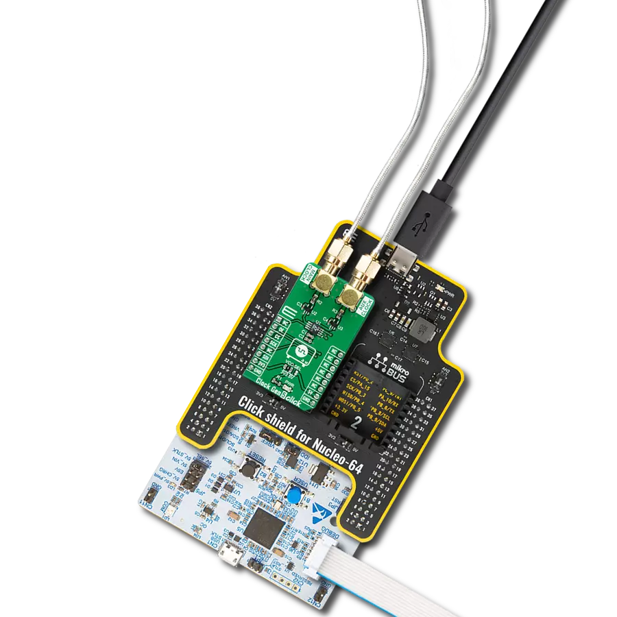
Start by selecting your development board and Click board™. Begin with the Nucleo-64 with STM32F091RC MCU as your development board.


Software Support
Library Description
This library contains API for PLL Click driver.
Key functions:
pll_set_clock_output- This function settings clock outputpll_set_pll_4x- This function settings PLL x4pll_set_pll_6x- This function settings PLL x6
Open Source
Code example
The complete application code and a ready-to-use project are available through the NECTO Studio Package Manager for direct installation in the NECTO Studio. The application code can also be found on the MIKROE GitHub account.
/*!
 * \file
 * \brief PLL Click example
 *
 * # Description
 * This app sets PLL signals.
 *
 * The demo application is composed of two sections :
 *
 * ## Application Init
 * Initializes device.
 *
 * ## Application Task
 * Every 2 seconds, the PLL increases the input clock from min (x2) to max (x8) level.
 *
 * \author MikroE Team
 *
 */
// ------------------------------------------------------------------- INCLUDES

#include "board.h"
#include "log.h"
#include "pll.h"

// ------------------------------------------------------------------ VARIABLES

static pll_t pll;
static log_t logger;

// ------------------------------------------------------ APPLICATION FUNCTIONS

void application_init ( void )
{
    log_cfg_t log_cfg;
    pll_cfg_t cfg;

    /**
     * Logger initialization.
     * Default baud rate: 115200
     * Default log level: LOG_LEVEL_DEBUG
     * @note If USB_UART_RX and USB_UART_TX
     * are defined as HAL_PIN_NC, you will
     * need to define them manually for log to work.
     * See @b LOG_MAP_USB_UART macro definition for detailed explanation.
     */
    LOG_MAP_USB_UART( log_cfg );
    log_init( &logger, &log_cfg );
    log_info( &logger, "---- Application Init ----" );

    //  Click initialization.
    pll_cfg_setup( &cfg );
    PLL_MAP_MIKROBUS( cfg, MIKROBUS_1 );
    pll_init( &pll, &cfg );
    pll_set_clock_output( &pll, PLL_CLOCK_ENABLE );
}

void application_task ( void )
{
    log_printf( &logger, " PLL level: x2\r\n\n" );
    pll_set_pll_2x( &pll );
    Delay_ms ( 1000 );
    Delay_ms ( 1000 );
    log_printf( &logger, " PLL level: x3\r\n\n" );
    pll_set_pll_3x( &pll );
    Delay_ms ( 1000 );
    Delay_ms ( 1000 );
    log_printf( &logger, " PLL level: x3.125\r\n\n" );
    pll_set_pll_3_125x( &pll );
    Delay_ms ( 1000 );
    Delay_ms ( 1000 );
    log_printf( &logger, " PLL level: x4\r\n\n" );
    pll_set_pll_4x( &pll );
    Delay_ms ( 1000 );
    Delay_ms ( 1000 );
    log_printf( &logger, " PLL level: x5\r\n\n" );
    pll_set_pll_5x( &pll );
    Delay_ms ( 1000 );
    Delay_ms ( 1000 );
    log_printf( &logger, " PLL level: x5.3125\r\n\n" );
    pll_set_pll_5_3125x( &pll );
    Delay_ms ( 1000 );
    Delay_ms ( 1000 );
    log_printf( &logger, " PLL level: x6\r\n\n" );
    pll_set_pll_6x( &pll );
    Delay_ms ( 1000 );
    Delay_ms ( 1000 );
    log_printf( &logger, " PLL level: x6.25\r\n\n" );
    pll_set_pll_6_25x( &pll );
    Delay_ms ( 1000 );
    Delay_ms ( 1000 );
    log_printf( &logger, " PLL level: x8\r\n\n" );
    pll_set_pll_8x( &pll );
    Delay_ms ( 1000 );
    Delay_ms ( 1000 );
}

int main ( void )
{
    /* Do not remove this line or clock might not be set correctly. */
    #ifdef PREINIT_SUPPORTED
    preinit();
    #endif

    application_init( );

    for ( ; ; )
    {
        application_task( );
    }

    return 0;
}

// ------------------------------------------------------------------------ END
Additional Support
Resources
Category:Clock generator